

 Integrated Magnetic Power Module
Buck (Step-Down)-Low Voltage
Buck (Step-Down)-Medium Voltage
Boost (Step-Up)
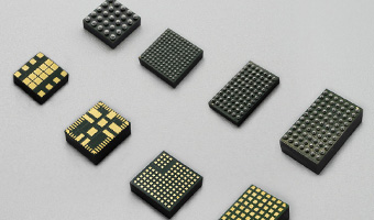
DC-DC Power Modules
Integrated Magnetic Power Module
Buck (Step-Down)-Low Voltage
Buck (Step-Down)-Medium Voltage
Boost (Step-Up)
DC-DC Power Modules
 Magnetically Integrated Power Module (SiP)
Buck (Step-Down)-Multiple Outputs
Buck (Step-Down)
Boost (Step-Up)
Magnetically Integrated Power Module (SiP)
Buck (Step-Down)-Multiple Outputs
Buck (Step-Down)
Boost (Step-Up)
 Customized DC-DC Converters
Tailored Power Modules: Precision Solutions for Your Unique Needs.
Contact Us Today to Discuss Your Project!
DC-DC Power Modules
Customized DC-DC Converters Explore DC-DC Converters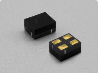
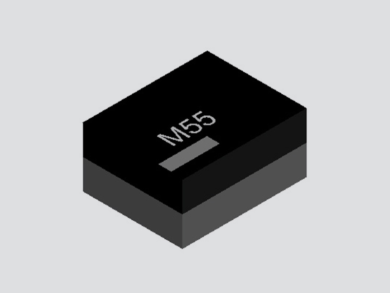
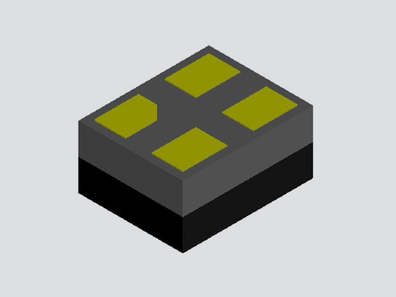
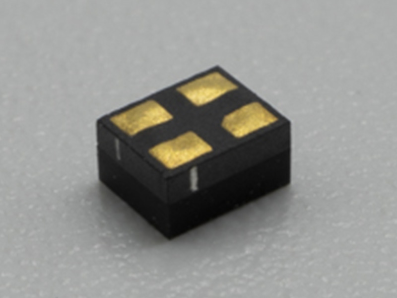
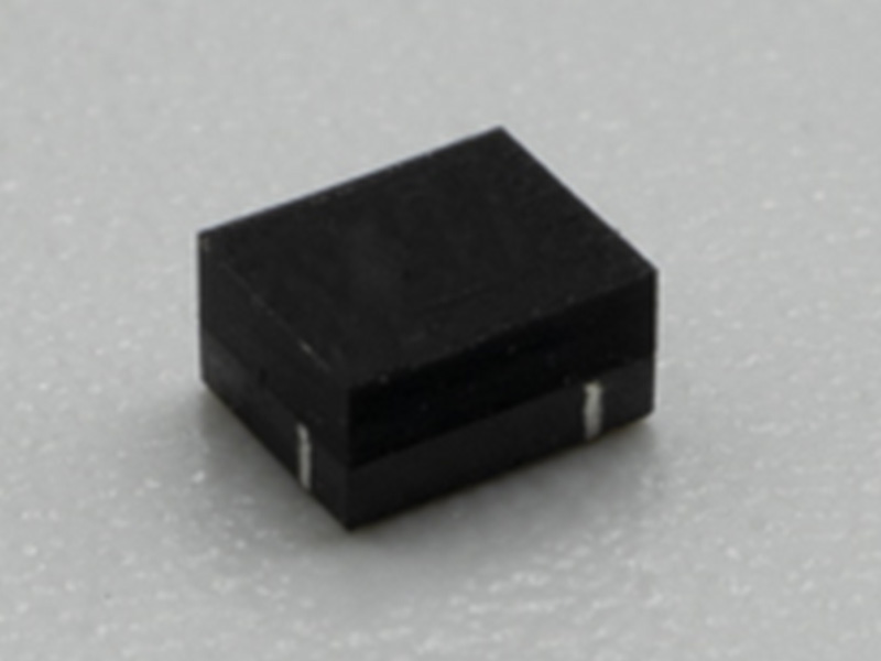
UDM22006 DC DC Integrated Magnetic Power Module ( Input 2.3V–5.5V, output 1.2V-3.3V )
Details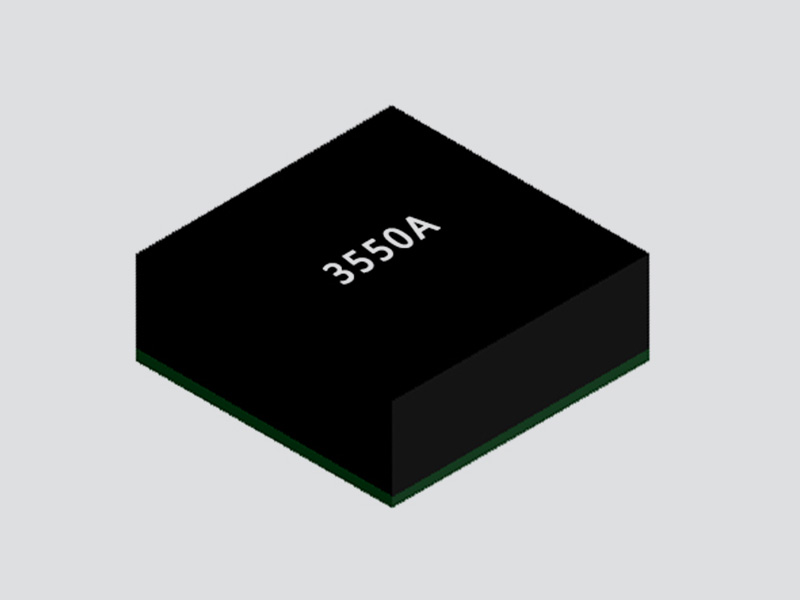
FHT3550 DC/DC Adjustable Buck Power Module ( 3.5V-40V Input, 1.0V-12.0V Output )
Details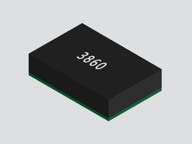
FHT3860 DC/DC Step-Down Buck Power Module ( 2.3V-5.5V Input, 0.5V-3.3V Output )
Details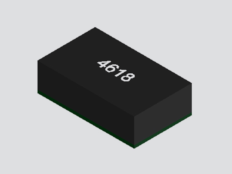
FHT4618 Integrated DC/DC Adjustable Buck Power Module ( 4.5V-24V Input, 0.6V-5.5V Output )
Details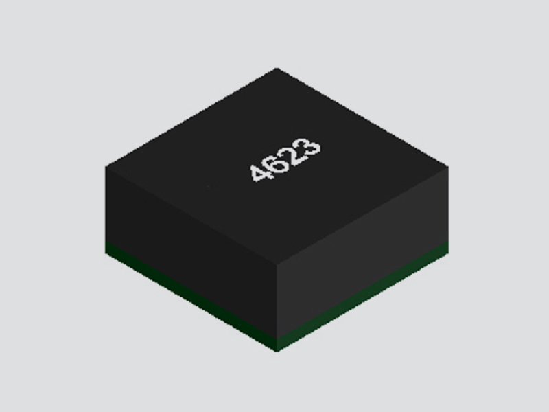
FHT4623 DC/DC Adjustable Buck Converter Power Module ( 4.2V-20V Input, 0.6V-5.5V Output )
Details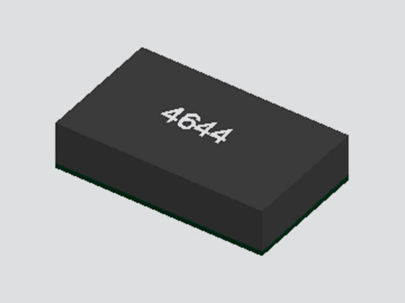
FHT4644 Ultra-Thin Multi-Channel DC/DC Buck Power Module ( 4.0V ~ 15V Input, 0.8V ~ 5.5V Output )
Details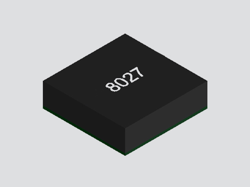
FHT8027C DC/DC Buck Converter Integrated Power Module ( 5V-60V Input, 2.5V-24V Output )
Details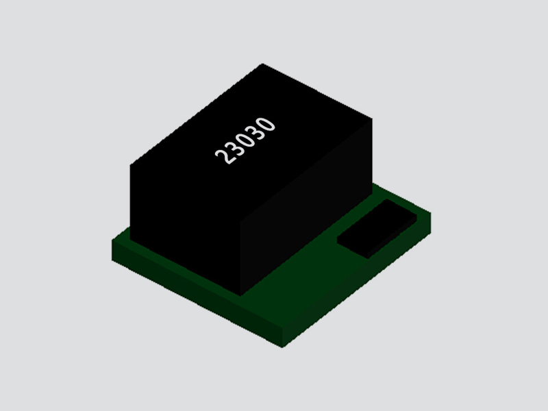
FHT23030 DC/DC Adjustable Buck Converter Module ( 4.5V–17V Input, 0.9V–6V Output )
Details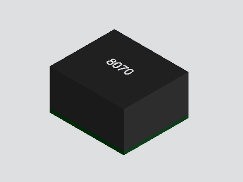
MPPM8070 DC/DC Adjustable Buck Converter Module ( Input 4.5V–18V, Output 0.6V-15V )
Details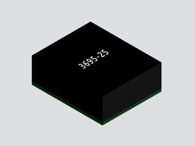
FHM3695 DC/DC Adjustable Buck Power Module ( 4V-16V Input, 0.6V-5.5V Output )
Details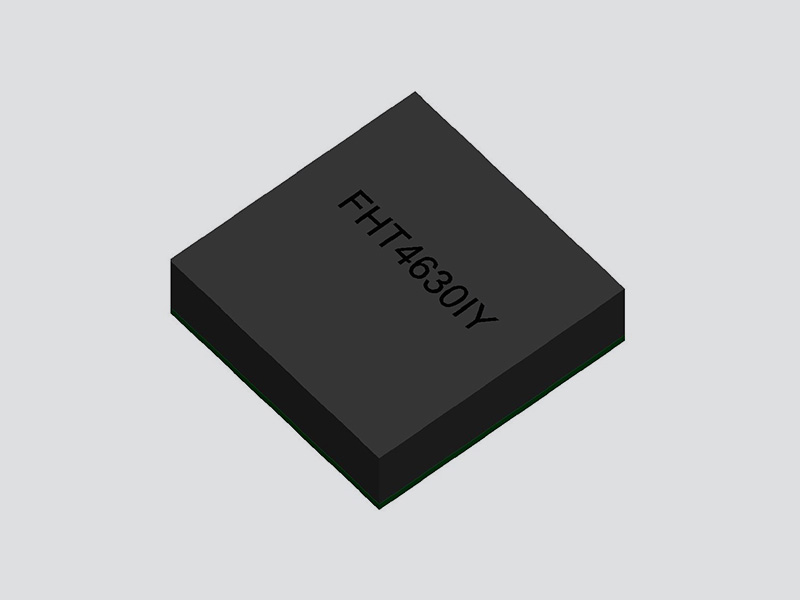
FHT4630 Dual-Channel DC/DC Adjustable Buck Converter Module ( 4.5V~15V Input, 0.6V ~ 1.8V Output )
Details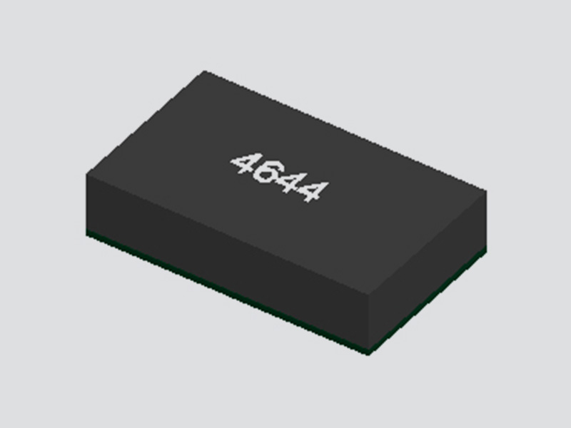
FHT4644C/D 4-Channel DC/DC Buck Power Module with Adjustable Outputs ( 4.5V-14V Input, 0.6V-5.5V Output )
Details
FHT4644F 4-Channel DC/DC Magnetically Integrated Buck Power Module (SiP) | 4.5V to 16V Input, 0.6V to 5.5V Output
Details
FHT4644H 4 Channel Integrated DC/DC Adjustable Buck Power Module ( 4.0V ~ 14V Input, 0.6V ~ 5.5V Output )
Details
FHT4644L 4-Channel Integrated Adjustable Buck DC/DC Power Module ( 4.0V ~ 15V Input, 0.8V ~ 5.5V Output )
Details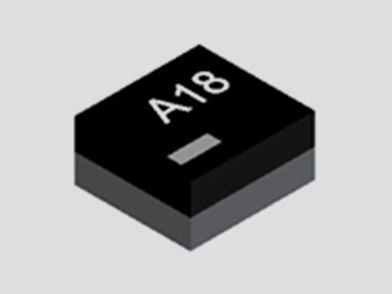
UDM2520I Integrated DC/DC Buck Step-Down Power Module ( 2.3V-5.5V Input, 0.8V-3.3V Output )
Details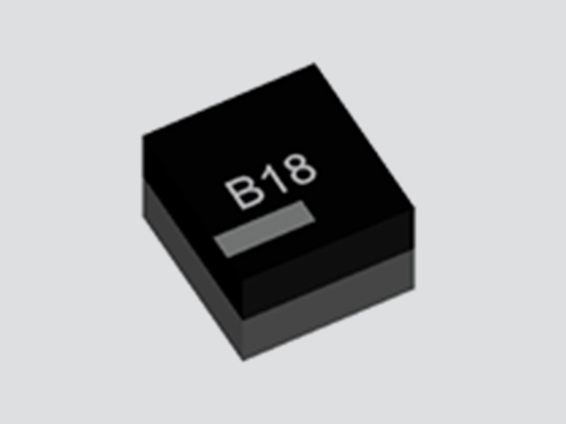
UDM2826I Integrated DC-DC Buck Step-Down Power Module ( 2.7V-5.5V Input, 1.0V-3.3V Output )
Details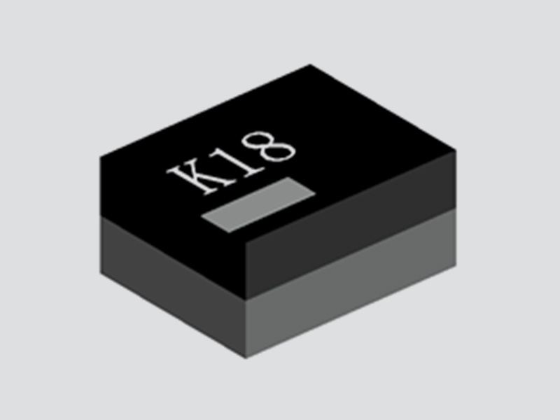
UDM22010 Integrated DC-DC Buck Step-Down Power Module ( 2.3V-5.5V Input, 1.2V-3.3V Output )
Details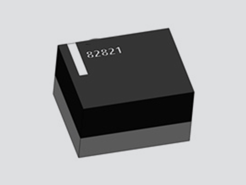
UDM82821 Integrated Magnetic DC-DC Buck Step-Down Power Module ( 2.3V-5.5V Input, 1.2V-3.3V Output )
Details
UDM82821adj Magnetically Integrated DC-DC Buck Power Module ( 2.5V-5.5V Input, 0.8V~4.0V Output )
Details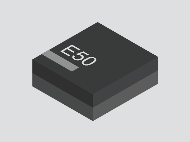
UDM81256 Integrated DC-DC Boost Power Module ( 2.5V-5.5V Input, Fixed 5V Output )
Details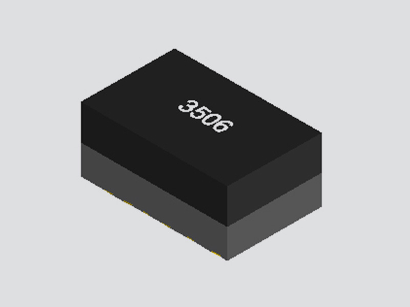
UDM3506 Integrated DC-DC Buck Step-Down Power Converter Module ( 4.7V-36V Input, 0.8V Output )
Details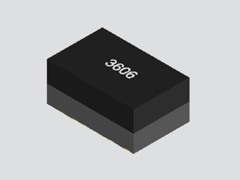
UDM3606 Integrated Medium Voltage DC-DC Buck Step-Down Power Module ( 4.5V-18V Input, 0.6V-5.5V Output )
Details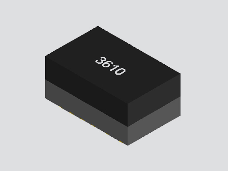
UDM3610 Integrated Medium Voltage DC-DC Buck Step-Down Power Supply Module ( 4.5V-18V Input, 0.6V-5.5V output )
DetailsIntegrated Power Inductor on Ferrite Ceramic Substrate
Ultra-small footprint(2.5mm×2.0mm)
Shielded structure, low EMI noise
Integrated capacitors in a single-package plastic encapsulation, providing high reliability for surface mount applications
Synchronous rectification technology achieves high efficiency
Automatic PFM/PWM Mode Switching Function
Uses low-ripple PFM mode under light load conditions
Achieves 2% voltage accuracy over the full load current range
Wide input voltage range:0.7V~5.5V
Adjustable Output Voltage: 1.8V~5.5V
Maximum Load Current:
Iout≥30mA(Vin≥0.7V ,Vout =5V)
Iout≥300mA(Vin≥2.7V ,Vout =5V)
Internal soft start, overcurrent protection, and overtemperature protection
Wireless Microphone
Portable Devices
Battery-Powered Equipment
The UDM92403 is a low-power boost DC-DC module suitable for space-constrained or noise-sensitive applications. The device features an inductor-embedded ferrite substrate, which reduces both radiated EMI noise and conducted noise. It uses a plastic integrated package to provide high mounting reliability while achieving an extremely small size (2.5mm × 2.0mm × 1.35mm / 1.10mm).
The external circuit can be used by adding input and output capacitors. The device offers low noise, easy usage, and reliable performance. The device smoothly switches between PFM (Pulse Frequency Modulation) and PWM (Pulse Width Modulation) modes based on the load current. Under light load conditions, it automatically switches to PFM mode to ensure low power consumption. Under heavy load conditions, it automatically switches to PWM mode to ensure low ripple. The device maintains excellent output voltage accuracy even in PFM mode, keeping the output voltage accuracy within ±2% over the entire load current range.
When Vin > Vout, the switch duty cycle is 100%, and the device enters bypass mode.
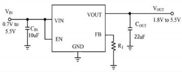
Note: Recommended Cin : 10μF/6.3V, Recommended Cout : 22μF/6.3V; Add more capacitance can decrease the ripple.
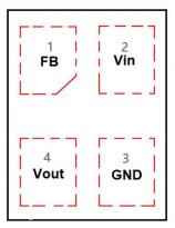
Pin | Symbol | Description |
1 | FB | Output voltage adjustment pin. Connect a voltage-setting resistor with a precision of 1% or better to GND. |
2 |
Vin | Positive input voltage. Provides power input to the internal power circuits and control circuits. The operating voltage range is 0.7V to 5.5V. The capacitor should be placed as close as possible to the module's Vin pin, and wide traces and multiple vias should be used wherever possible. |
3 | GND | Ground Pin |
4 | Vout | Regulated output pin. Connect the output load between this pin and GND. |
Absolute Maximum Ratings | Conditions | Minimum Value | Nominal Value | Maximum Value | Units |
VIN, EN | -0.3 | 6 | V | ||
vsw | -0.3 | 6 | V | ||
VFB Pin Voltage | -0.3 | 6 | V | ||
VOUT | 1.8 | 6 | V | ||
Storage Temperature | -65 | +150 | ℃ | ||
Electrical characteristics | Conditions | Minimum Value | Nominal Value | Maximum Value | Units |
Input Voltage Range | 0.7 | 5.5 | V | ||
Input Undervoltage Lockout Threshold (Rising) | 0.6 | 0.7 | V | ||
Minimum Start-Up Voltage | 0.4 | V | |||
Quiescent current | VEN =3.7V, VFB =VREF x 105% | 4.5 | μA | ||
Shutdown current | Vin=3.7V,VEN=GND | 0.5 | 1.4 | μA | |
Switching Frequency | 3 | MHz | |||
Efficiency | Vin =3V ,Vout =3.3V ,Iout=0.05A | 93.5 | % | ||
EN Threshold (On) | 1.2 | V | |||
EN Threshold (Off) | 0.4 | V | |||
Maximum Duty Cycle | 100 | % | |||
Minimum On-Time | 80 | ns | |||
Soft-Start Time | 0.6 | ms | |||
FB Voltage | 0.98 | 1 | 1.02 | V | |
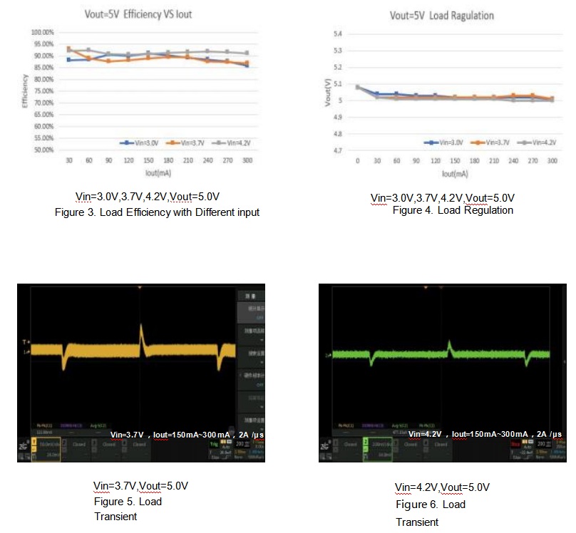
Line regulation | Vout=5V ,2.4V < Vin< 4.2V ,ILOAD = 0.3A | ±2 | % | ||
Load regulation | Vin=3.7V ,Vout=5V,0A < ILOAD ≤ 0.3A | ±2 | % | ||
Ripple and noise | Vin =3.7V ,Vout =5V ,Iout=0.15A, Cout=22uF, Bandwidth: 20MHz | 25 | mV | ||
Dynamic load response | 50-100% ILOAD ,di/dt=2A/μS Cout=22 uF |
150 |
mV |
Electrical Characteristics(continued)
Structural Characteristics | Conditions | Minimum Value | Nominal Value | Maximum Value | Units |
Dimensions | 2.5×2.0×1.35Max 2.5×2.0×1.10Max | mm | |||
Weight | 0.024 | g | |||
Environmental Adaptability | Conditions | Minimum Value | Nominal Value | Maximum Value | Units |
Operating Temperature (Case Temperature) | -40 | 125 | ℃ | ||
High-Temperature Storage (Ambient Temperature) | +125℃ , 48h | 125 | ℃ | ||
High-Temperature Operation (Ambient Temperature) | +85℃ , 24h; Low Input Voltage, Nominal Input Voltage, High Input Voltage, 8 hours; Vin =60V ,Vout =12V ,Iout=2.4A |
85 | ℃ | ||
Low-Temperature Storage (Ambient Temperature) | -55℃ , 24h | -55 | ℃ | ||
Low-Temperature Operation (Ambient Temperature) | -40℃ , 24h; Low Input Voltage, Nominal Input Voltage, High Input Voltage, 8 hours; | -40 | ℃ | ||
Humid Heat | High-Temperature and High-Humidity Stage: 60℃ , 95%; Low-Temperature and High-Humidity Stage: 30℃ , 95%; 10 cycles of 24h each |
30 |
60 | ℃ | |
Temperature Shock | High Temperature: 125℃, Low Temperature: -55℃, High and low temperatures of one hour each for a cycle, a total of 32 cycles of testing | -55 | 125 | ℃ |
Note: Stress above the values listed in the "Absolute Maximum Ratings" section may cause permanent damage to the device. Exposure to any absolute maximum rating condition for extended periods may affect the reliability and lifespan of the device.
Unless otherwise noted, test conditions are T(environment) = 25℃
Summary
The UDM92403 is a DC-DC boost power module with synchronous rectification control. It integrates an inductor, power MOSFETs, and filtering capacitors. The UDM92403 provides a complete power solution, requiring only a few external passive components to achieve a wide input voltage range of 0.7V to 5.5V, adjustable output voltage, and excellent load and line regulation.
The UDM92403 includes comprehensive protection features such as Over Current Protection (OCP), Short Circuit Protection (SCP), Over Voltage Protection (OVP), Under Voltage Protection (UVP), and Over Temperature Protection (OTP). These protections minimize the need for external components, making the UDM92403 highly efficient and easy to use.
Internal Soft-Start (SS)
The soft start function is designed to prevent overvoltage at the output during the module's startup process. The UDM92403 has an integrated soft start feature: when the EN pin is connected to a high voltage, the UDM92403 begins to start. Initially, the device operates at the boundary between Discontinuous Conduction Mode (DCM) and Continuous Conduction Mode (CCM), with the peak inductor current limited to around 200mA. When the output voltage charges to approximately 1.6V or higher, the device begins to operate in hysteretic current mode. The soft start function helps reduce inrush current during startup. Once Vout reaches the target value, the soft start phase ends, and the peak current is determined by the output of the internal error amplifier, which compares the feedback of the output voltage with the internal reference voltage.
Startup and Shutdown
If both Vin and VEN exceed their respective thresholds, the module starts. The internal reference voltage circuit starts first, generating a stable reference voltage. Subsequently, the internal regulator is enabled, providing a stable power supply to the rest of the circuit.
Three conditions can cause the chip to shut down: Vin being too low, VEN being too low, and over-temperature shutdown protection. During the shutdown process, the signal loop is first blocked to prevent false triggering. Subsequently, the COMP voltage and internal power supply are pulled down. The open-drain driver is not affected by this shutdown command.
Overcurrent Protection and Short Circuit (OCP)
The UDM92403 features overcurrent protection. If the inductor peak current reaches the current limit threshold, the main switch turns off, preventing further increase in input current. In this situation, the output voltage will drop until a power balance is achieved between the input and output.
Output Short-Circuit Protection
In the event of a ground short circuit, the short-circuit current is limited to around 85mA. After the short-circuit condition is removed, the UDM92403 will return to soft start and regulate the output voltage.
Overtemperature Shutdown Protection (OTP)
To prevent any damage caused by overheating, the UDM92403 stops switching when the internal chip temperature exceeds 150°C. Once the temperature falls below the threshold (typically 130°C), the module resumes operation.
Undervoltage Lockout Protection (UVLO)
When the input voltage drops below the typical UVLO (Undervoltage Lockout) threshold of 0.4V, the UVLO circuit stops the operation of the converter. The hysteresis voltage value is 200mV.
Output Voltage Setting
The module internally integrates a 510kΩ pull-up resistor. The output voltage can be adjusted by connecting an external pull-down resistor Rj to the FB pin. The reference calculation formula is as follows:
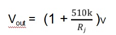
Table 1 provides recommended parameters for common output voltages.
Under normal circumstances, it is suggested to set the output voltage between 1.8V and 5.5V.
![]()
Side View
Top View Top View
(Scenpgraph)
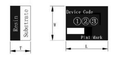
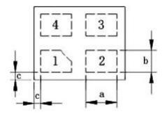
Symbol | Dimension (mm) |
L | 2.5±0.2 |
W | 2.0±0.2 |
T | 1.35Max or1. 1Max |
a | 0.85±0.1 |
b | 0.60±0.1 |
c | 0. 15±0.15 |
Soldering and Storage Precautions
Recommended Reflow Soldering Profile
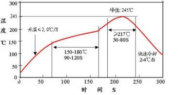
Note:
1.Due to the larger size of the module, do not place the module on the bottom side of the board during reflow soldering to avoid module drop.
2.For bulk and unpackaged products, store them in a dry box (relative humidity should be kept below 10%). For products that are still in their original packaging, store them in a dry box whenever possible.
3.Before mounting, moisture-sensitive products must be baked according to strict baking conditions: bake for more than 48 hours at 125°C.
Product Model | Input Voltage | Output Voltage | Output Current | Packaging | Product Grade |
UDM92403 IV#PBF | 0.7V~5.5V | 1.8V~5.5V | Ioutmax=300mA | 3000pcs/roll | Industrial Grade |
Product Model | Input Voltage | Output Voltage | Output Current | Packaging | Product Grade |
UDM92403 MV#PBF | 0.7V~5.5V | 1.8V~5.5V | Ioutmax=300mA | 3000pcs/roll | Military Grade |
| Item | Description | Reel/Tray | Pcs/Roll | G.W | N.W | QTY/Carton | Package Size |
| UDM92403 | 0.7V~5.5V Input, 1.8V-5.5V Output, Integrated DC-DC Boost Step-Up Power Module, Efficiency up to 93% |
| 3,000pcs | 0.25kgs | 0.07kgs | 3,000pcs | 150*150*50mm |
Discover all the technical specifications by downloading the datasheet today.
| Part Number |
Output Current
(A) |
Input Voltage
(V) |
Output Voltage
(V) |
Dimensions(mm) |
Maximum
Efficienc |
Factory Pack
Quantity |
Footprint 3D | Datasheet | Sample |
| UDM2520I | 0.6A | 2.3V ~ 5.5V | 0.8V~3.3V | 2.5mm × 2mm x 1.1mm | 94% | 3,000pcs |  |
 |
|
| UDM22006 | 0.6A | 2.3V~5.5V | 1.2V~3.3V | 2.5mm x 2mm x 1.1mm | 95% | 3,000pcs | |
|
|
| UDM22010 | 1A | 2.3V ~ 5.5V | 1.2V ~ 3.3V | 2.5mm x 2mm x 1.1mm | 95% | 3,000pcs | |
|
|
| UDM82821adj | 1A | 2.5V~5.5V | 0.8V~4V | 2.5mm × 2mm x 1.1mm | 95% | 3,000pcs | |
|
|
| UDM82821 | 1.2A | 2.3V~5.5V | 1.2V~3.3V | 2.5mm × 2mm x 1.1mm | 95% | 3,000pcs | |
|
|
| UDM2826I | 1.5A | 2.7V ~ 5.5V | 1V ~ 3.3V | 2.8mm × 2.6mm x 1.1mm | 93% | 3,000pcs | |
|
|
| UDM3606 | 0.6A | 4.5V-18V | 0.6V-5.5V | 5mm×3.2mm×2.2mm | 95% | 3,000pcs | |
|
|
| UDM3506 | 0.6A | 4.7V-36V | 0.8V | 5mm×3.2mm×2.2mm | 88% | 3,000pcs | |
|
|
| UDM3610 | 1.2A | 4.5V~18V | 0.6V~5.5V | 5mm×3.2mm×2.2mm | 95% | 3,000pcs | |
|
|
| UDM92403 | 0.3A | 0.7V~5.5V | 1.8V~5.5V | 2.5mm×2mm x 1.1mm | 93% | 3,000pcs | |
|
|
| UDM81256 | 1A | 2.5V ~ 5.5V | 5V | 2.8mm×2.6mm×1.35mm(1.1mm) | 95% | 3,000pcs | |
|
|
| FHT4644 | 4A | 4.0V ~ 15V | 0.8V ~ 5.5V | 9mm x 15mm x 4.32mm | 92% | 500pcs | |
|
|
| FHT4644H | 4A | 4.0V ~14V | 0.6V ~ 5.5V | 9mmx15mmx4.32mm | 92% | 500pcs | |
|
|
| FHT4644C/D | 4A | 4.5V-14V | 0.6V-5.5V | 9mmx15mmx4.32mm | 92% | 500pcs | |
|
|
| FHT4644F | 4A | 4.5V ~ 16V | 0.6V ~ 5.5V | 9.0mmx15mmx4.32mm | 92% | 500pcs | |
|
|
| FHT4644L | 4A | 4.0V ~15V | 0.8V ~ 5.5V | 9mmx15mmx1.82mm | 92% | 500pcs | |
|
|
| FHT4630 | 18A+18A | 4.5V~15V | 0.6V ~ 1.8V | 16mm × 16mm × 5.01mm | 94% | 500pcs | |
|
|
| FHT3860 | 6A | 2.3V-5.5V | 0.5V-3.3V | 4mm x 6mm x 1.6mm | 94% | 500pcs | |
|
|
| FHM3695-25 | 20A | 4V-16V | 0.6V-5.5V | 10mm × 12mm ×4.32mm | 95% | 500pcs | |
|
|
| FHT4623 | 3A | 4.2V-20V | 0.6V-5.5V | 6.75mm x 6.75mm x 2.95mm | 95% | 500pcs | |
|
|
| MPPM8070 | 2A | 4.5V-18V | 0.6V-15V | 8mm×7mm × 4.32(2.5mm) | 93% | 500pcs | |
|
|
| FHT4618 | 6A | 4.5V-24V | 0.6V-5.5V | 15mm×9mm×4.32mm | 95% | 500pcs | |
|
|
| FHT23030 | 3A | 4.5V-17V | 0.9V-6V | 3mm×2.8mm×1.4mm | 94% | 500pcs | |
|
|
| FHT3550 | 5A | 3.5V-40V | 1.0V-12.0V | 12mm x 12mm x 4.32mm | 95% | 500pcs | |
|
|
| FHT8027C | 4A | 5V-60V | 2.5V-24V | 15mm×15mm×4.32mm | 95% | 500pcs | |
|

Data Centers and Server Farms

Medical Devices

Aerospace and Defense

Automotive Electronics

Industrial and Automation

Consumer Electronics
Telecommunications and Networking