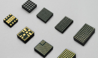


 Integrated Magnetic Power Module
Buck (Step-Down)-Low Voltage
Buck (Step-Down)-Medium Voltage
Boost (Step-Up)
DC-DC Power Modules
Integrated Magnetic Power Module
Buck (Step-Down)-Low Voltage
Buck (Step-Down)-Medium Voltage
Boost (Step-Up)
DC-DC Power Modules
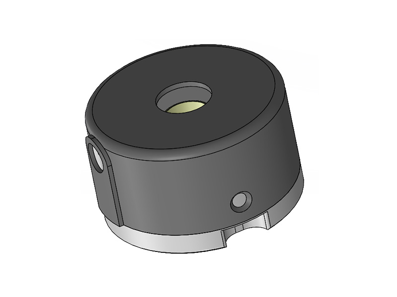
 Magnetically Integrated Power Module (SiP)
Buck (Step-Down)-Multiple Outputs
Buck (Step-Down)
Boost (Step-Up)
Magnetically Integrated Power Module (SiP)
Buck (Step-Down)-Multiple Outputs
Buck (Step-Down)
Boost (Step-Up)
 Customized DC-DC Converters
Tailored Power Modules: Precision Solutions for Your Unique Needs.
Contact Us Today to Discuss Your Project!
DC-DC Power Modules
Customized DC-DC Converters Explore DC-DC Converters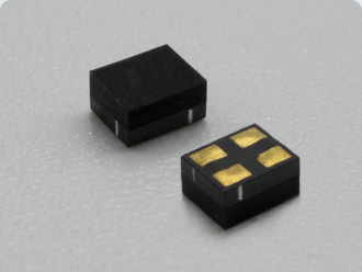
UDM22006 DC DC Integrated Magnetic Power Module ( Input 2.3V–5.5V, output 1.2V-3.3V )
Details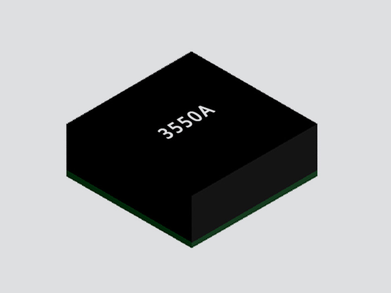
FHT3550 DC/DC Adjustable Buck Power Module ( 3.5V-40V Input, 1.0V-12.0V Output )
Details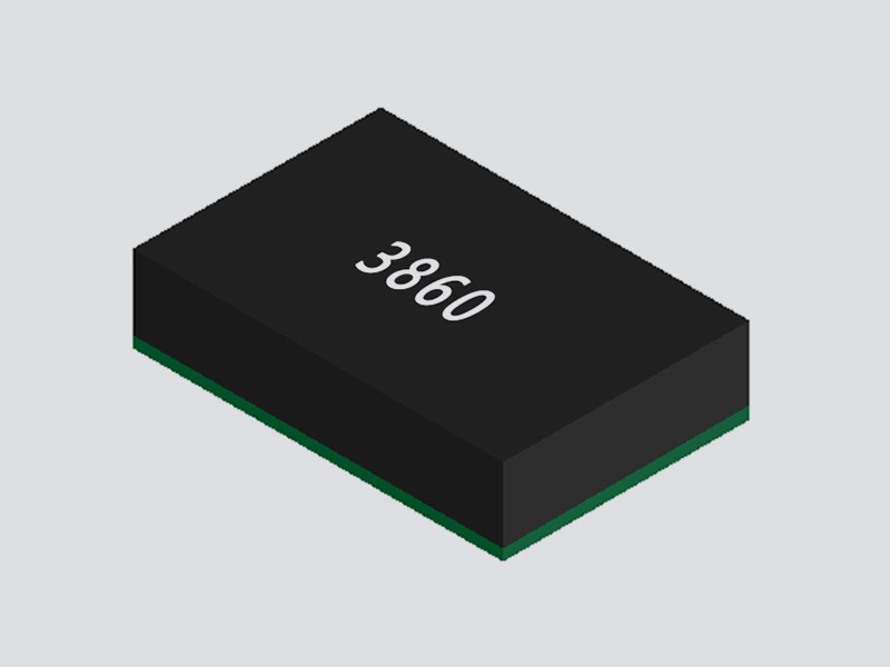
FHT3860 DC/DC Step-Down Buck Power Module ( 2.3V-5.5V Input, 0.5V-3.3V Output )
Details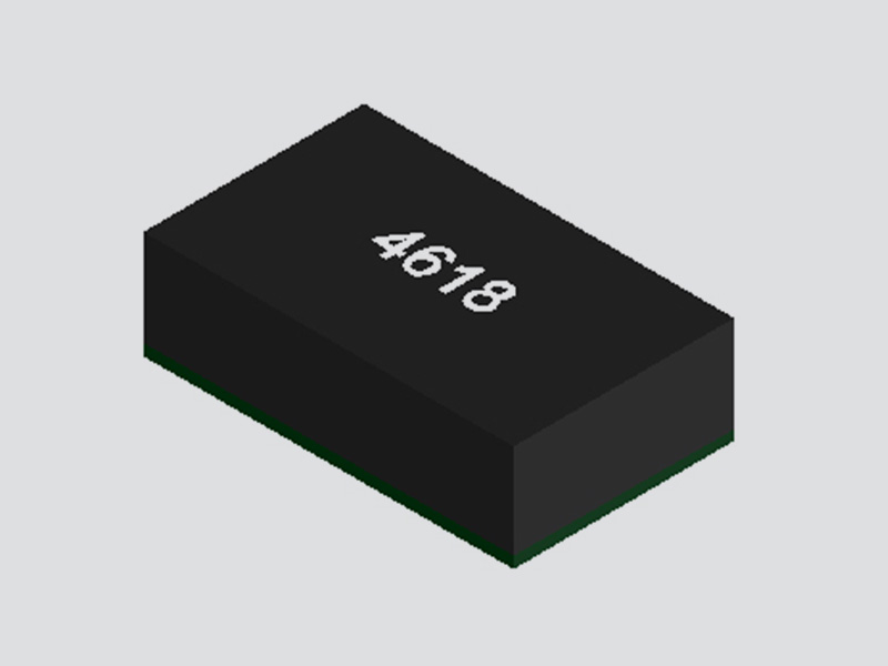
FHT4618 Integrated DC/DC Adjustable Buck Power Module ( 4.5V-24V Input, 0.6V-5.5V Output )
Details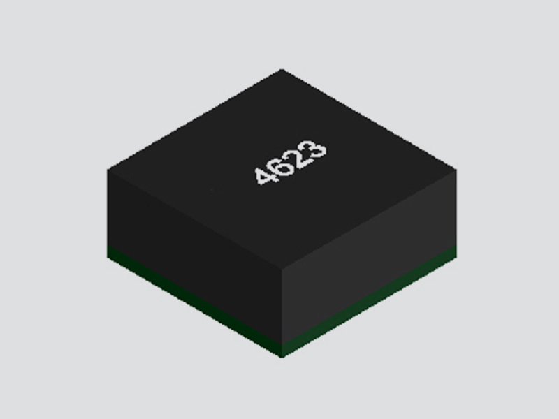
FHT4623 DC/DC Adjustable Buck Converter Power Module ( 4.2V-20V Input, 0.6V-5.5V Output )
Details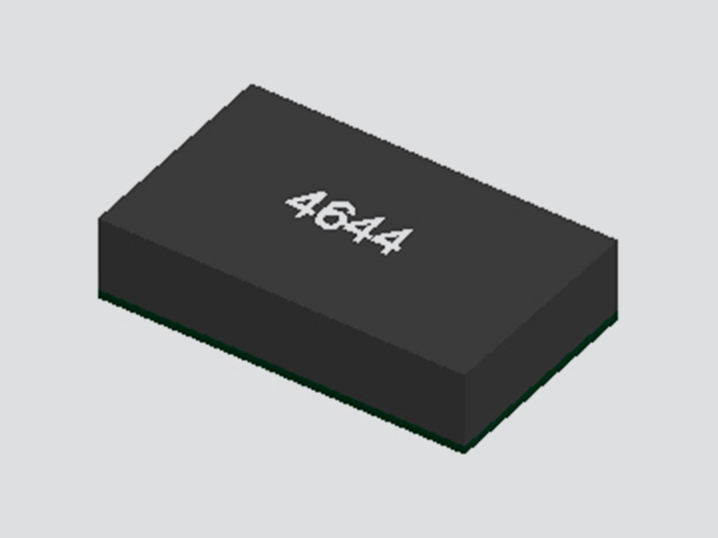
FHT4644 Ultra-Thin Multi-Channel DC/DC Buck Power Module ( 4.0V ~ 15V Input, 0.8V ~ 5.5V Output )
Details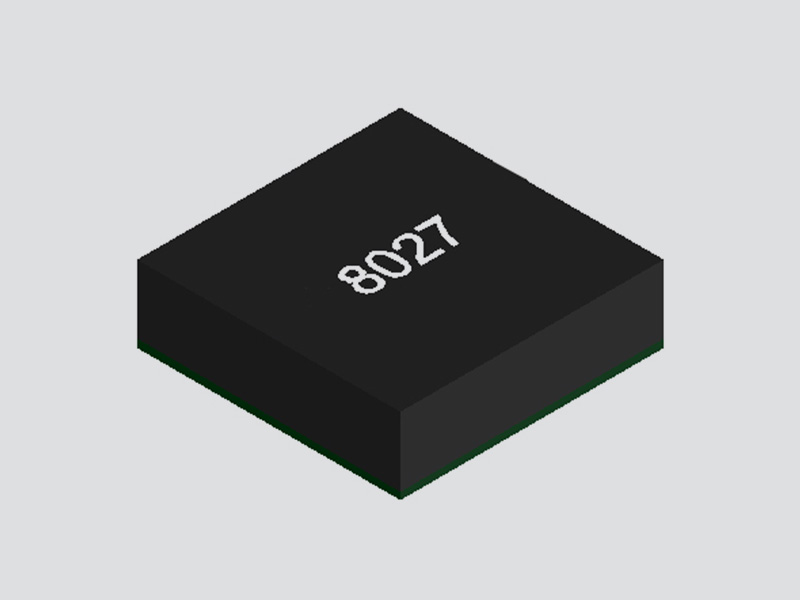
FHT8027C DC/DC Buck Converter Integrated Power Module ( 5V-60V Input, 2.5V-24V Output )
Details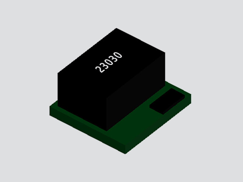
FHT23030 DC/DC Adjustable Buck Converter Module ( 4.5V–17V Input, 0.9V–6V Output )
Details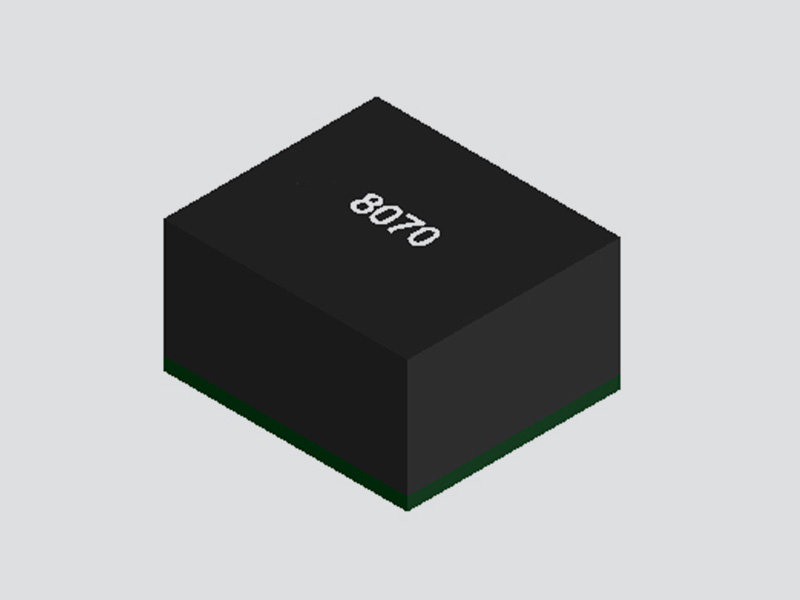
MPPM8070 DC/DC Adjustable Buck Converter Module ( Input 4.5V–18V, Output 0.6V-15V )
Details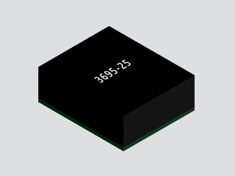
FHM3695 DC/DC Adjustable Buck Power Module ( 4V-16V Input, 0.6V-5.5V Output )
Details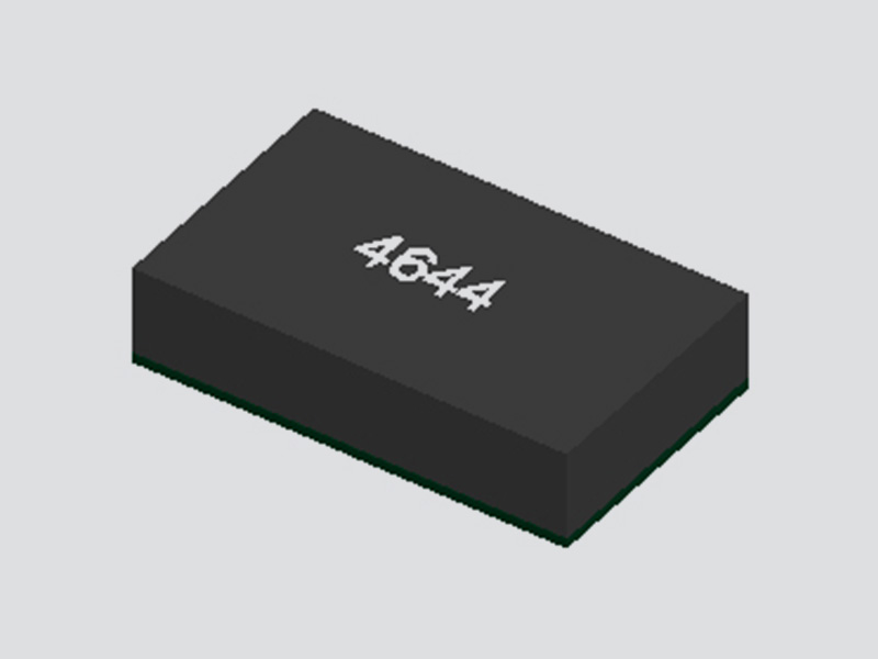
FHT4644C/D 4-Channel DC/DC Buck Power Module with Adjustable Outputs ( 4.5V-14V Input, 0.6V-5.5V Output )
Details
FHT4644F 4-Channel DC/DC Magnetically Integrated Buck Power Module (SiP) | 4.5V to 16V Input, 0.6V to 5.5V Output
Details
FHT4644H 4 Channel Integrated DC/DC Adjustable Buck Power Module ( 4.0V ~ 14V Input, 0.6V ~ 5.5V Output )
Details
FHT4644L 4-Channel Integrated Adjustable Buck DC/DC Power Module ( 4.0V ~ 15V Input, 0.8V ~ 5.5V Output )
Details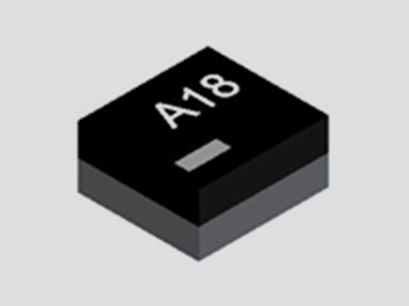
UDM2520I Integrated DC/DC Buck Step-Down Power Module ( 2.3V-5.5V Input, 0.8V-3.3V Output )
Details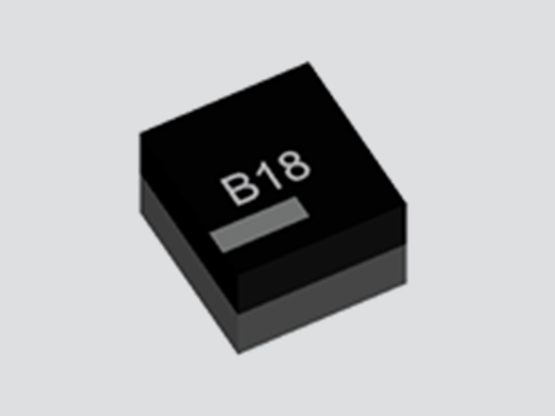
UDM2826I Integrated DC-DC Buck Step-Down Power Module ( 2.7V-5.5V Input, 1.0V-3.3V Output )
Details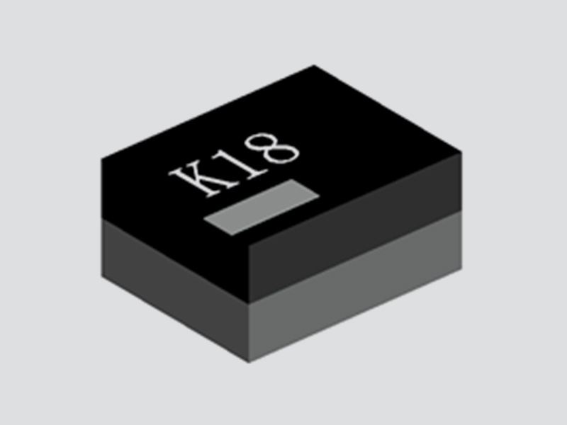
UDM22010 Integrated DC-DC Buck Step-Down Power Module ( 2.3V-5.5V Input, 1.2V-3.3V Output )
Details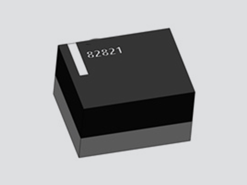
UDM82821 Integrated Magnetic DC-DC Buck Step-Down Power Module ( 2.3V-5.5V Input, 1.2V-3.3V Output )
Details
UDM82821adj Magnetically Integrated DC-DC Buck Power Module ( 2.5V-5.5V Input, 0.8V~4.0V Output )
Details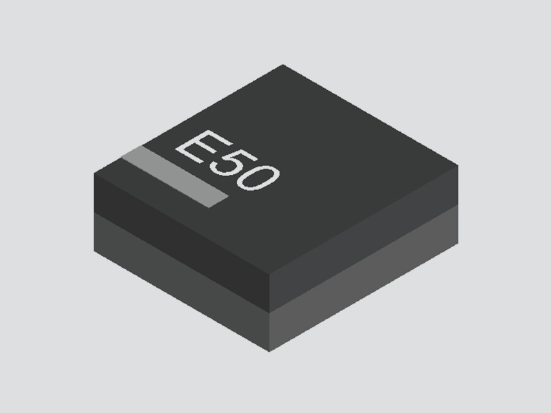
UDM81256 Integrated DC-DC Boost Power Module ( 2.5V-5.5V Input, Fixed 5V Output )
Details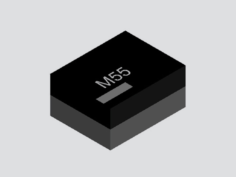
UDM92403 Integrated DC-DC Boost Step-Up Power Module ( 0.7V-5.5V Input, Adjustable 1.8V-5.5V Output )
Details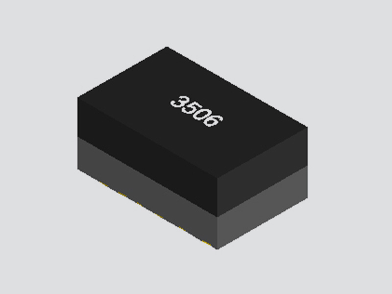
UDM3506 Integrated DC-DC Buck Step-Down Power Converter Module ( 4.7V-36V Input, 0.8V Output )
Details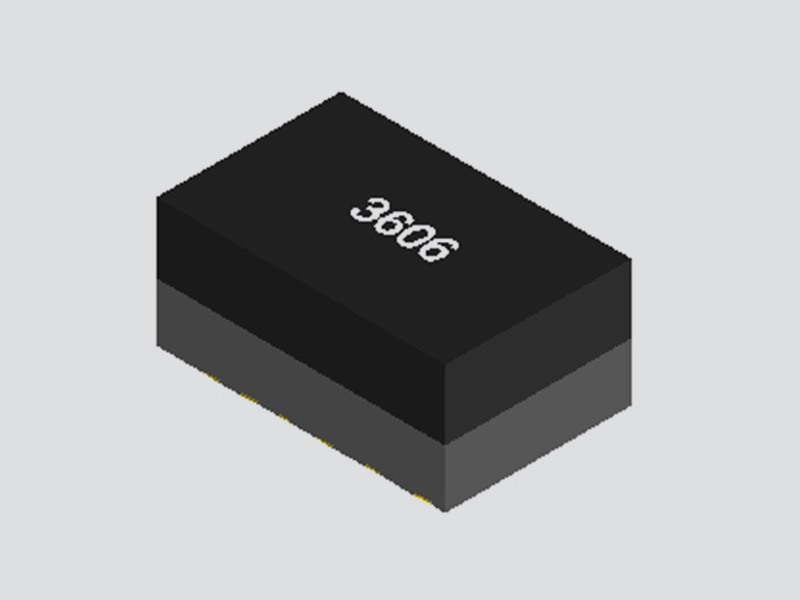
UDM3606 Integrated Medium Voltage DC-DC Buck Step-Down Power Module ( 4.5V-18V Input, 0.6V-5.5V Output )
Details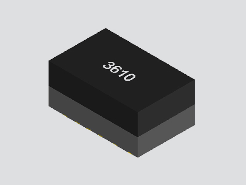
UDM3610 Integrated Medium Voltage DC-DC Buck Step-Down Power Supply Module ( 4.5V-18V Input, 0.6V-5.5V output )
DetailsTwo 18A or single 36A outputs
Wide input voltage range: 4.5V~15V
Output voltage: 0.6 ~ 1.8V range adjustable
Differential Remote Sampling Amplifier
Adjustable switching frequency
With external frequency synchronization
Up to 8 phases can be connected in parallel with amaximum current of 144A.
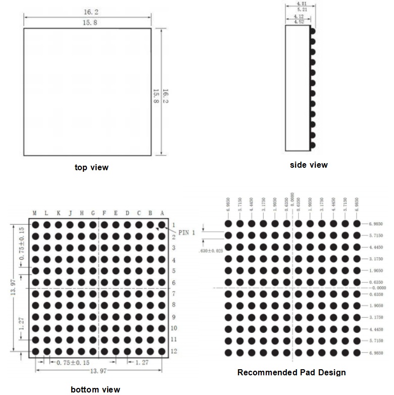
Size: 16mm × 16mm × 4.32mm (LGA)
16mm × 16mm × 5.01mm (BGA)
Telecommunications and network equipment
Industrial equipment
Servers and computing
FPGA / ASIC AI and Data Mining
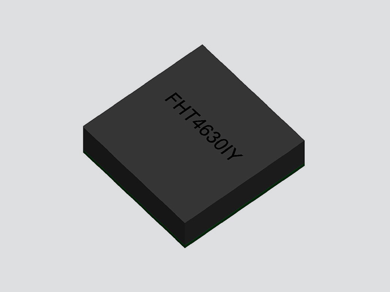
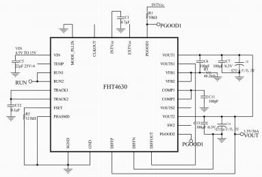
The FHT4630 is a dual-channel 18A or single-channel 36A output switch-mode step-down DC-DC voltage regulator module that integrates a power controller, power MOSFETs, inductors, and other peripheral components internally. The input voltage range of the FHT4630 is 4.5V to 15V, and it supports two independently adjustable outputs ranging from 0.6V to 1.8V or dual-channel parallel output by adjusting an external resistor respectively. Based on its high-efficiency design, the FHT4630 requires only a small amount of input and output capacitance to provide up to 18A of output current per channel.
The FHT4630 offers a complete power solution with excellent load regulation and line regulation. It operates efficiently over a wide load range and can be paralleled to provide higher load currents.
The FHT4630 features comprehensive protection functions, including over-current protection (OCP), over-voltage protection (OVP), under-voltage protection (UVP), and over-temperature protection (OTP). The FHT4630 minimizes the use of external components and comes in package sizes of 16mm×16mm×4.32mm (LGA) and 16mm×16mm×5.01mm (BGA).
PIN CONFIGURATION
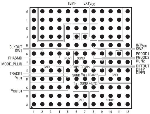
Pin | Symbol | Description |
A1-A5, B1-B5, C1-C4 | VOUT1 | Power output 1 pin. Connect the output load between VOUT1 and GND. A filter capacitor needs to be placed between VOUT1 and GND. |
A6-A7, B6-B7, D1-D4, D9-D12, E1-E4, E10- E12, F1-F3, F10-F12, G1, G3, G10, G12, H1- H7, H9-H12, J1, J5, J8, J12, K1, K5-K8, K12, L1, L12, M1 , M12 |
GND |
Power ground pins for inputs and outputs. |
A8-A12, B8-B12, C9-C12 |
VOUT2 | Power Output 2 pin. Connect the output load between VOUT2 and GND. A filter capacitor needs to be placed between VOUT2 and GND. |
C5, C8 | VOUTS1, VOUTS2 | Output voltage sampling pin. This pin is internally connected via a resistor to the corresponding feedback pin (VFB1/2). This pin can be connected directly to the output (VOUT). When a remote sampling amplifier is used, it can be connected to the DIFFOUT pin. When used in parallel, connect either VOUTS1 and VOUTS2 to the DIFFOUT pin or the VOUT pin. This pin cannot be left open. |
PIN CONFIGURATION
Pin | Symbol | Description |
C6 | fSET | Frequency setting pin. This pin outputs 10μA of current. Connecting a resistor from this pin to GND will generate a voltage across the resistor that will determine the switching frequency. A DC voltage can also be connected to this pin to set the operating frequency. |
C7, D6, G6-G7, F6-F7 | SGND | Signal ground pins. All weak signals for control are routed back to the module through this set of pins. In the application, a single connection is made to the GND terminal of the output capacitor. |
D5, D7 |
VFB1, VFB2 | The input of the error amplifier for the corresponding channel. Inside the module, this pin is connected to VOUTS through a 60.4kΩ resistor. Resistors of different values are connected between this pin and GND to set different output voltages. When used in parallel, connect VFB1 and VFB2, and then connect a resistor to GND. |
E5, D8 | TRACK1, TRACK2 | Output voltage tracking and soft-start pins. Each channel provides 1.3μA current. |
E6, E7 | COMP1, COMP2 | Current control threshold and error amplifier compensation terminals. When used in parallel , connect E6 and E7. |
E8 | DIFFP | Remote Sampling Error Amplifier In-Phase Input. Connect this pin to the remote sampling positive terminal of the output voltage. |
E9 | DIFFN | Remote Sampling Error Amplifier Inverting Input. Connect this pin to the remote sampling GND terminal of the output voltage. |
F4 | MODE_PLLIN | Operating mode selection and external phase synchronization detection pin. When this pin is connected to SGND, both channels are in forced continuous mode (FCC); when it is connected to the INTVCC pin, it is in pulse-hopping mode; and when it is left open, it is in pulse burst mode. See Application Information for details. |
F5, F9 | RUN1, RUN2 | Enable control pin. Connecting a voltage of 1.2V or more will turn on the corresponding channel. |
F8 | DIFFOUT | Internal remote sampling error amplifier output. Connects to VOUTS that use remote sampling channels. |
G2, G11 | SW1, SW2 | Switching node for measurement. Can be connected to an R-C network to reduce or eliminate ringing, or can be left open. See application information for details. |
G4 | PHASMD | Phase Adjustment Pin. Connected to SGND, INTVcc, or null, the corresponding CLOCK phase difference is 60°, 120°, or 90°, in that order. |
G5 | CLKOUT | Clock output pin with phase control. Used for phase interleaving control when multiple modules are connected in parallel. |
G9, G8 | PGOOD1, PGOOD2 | Output voltage status indication pin. When the output voltage exceeds ±10% of the rated value, this pin will be pulled to ground. |
H8 | INTVCC | Internal 5V regulated output. It mainly supplies power for internal control circuits and gate driver circuits. Connect a 4.7μF low ESR ceramic chip capacitor between this pin and ground. When either RUN1 or RUN2 is active, INTVcc will also be active. |
J6 | TEMP | NC. |
J7 | EXTVCC | External power input pin. When the external input voltage is greater than 4.7V, the external input power function will be enabled. When the input voltage VIN is 5V, connect this pin to VIN. |
M2-M11, L2-L11, J2-J4, J9-J11, K2- K4, K9-K11 |
VIN |
Power input pin. Connect the input voltage between VIN and GND. Requires a decoupling capacitor to be placed between VIN and GND. |
Absolute Maximum Ratings | Condition | Minimum Value | Nominal Value | Maximum Value | Unit |
VIN | -0.3 | 16 | V | ||
VOUT1, VOUT2, VOUTS1, VOUTS2 | -0.3 | 6 | V | ||
PGOOD1, PGOOD2, RUN1, RUN2, INTVCC, EXTVCC | -0.3 | 6 | V | ||
VSW | -1 | 16 | V | ||
DIFFP, DIFFN, DIFFOUT, PHASMD | -0.3 | INTVCC | V | ||
COMP1, COMP2, VFB1, VFB2 | -0.3 | 2.7V | V | ||
Storage temperature | -55 | +125 | ℃ | ||
Input Characteristics | Condition | Minimum Value | Nominal Value | Maximum Value | Unit |
Input Voltage Range | 4 | 15 | V | ||
Input surge current (startup) | IOUT = 0A, CIN = 22µF × 3, CSS = 0.1µF, COUT = 100µF × 3, VOUT1 = 1.5V, VOUT2 = 1.5V, VIN = 12V | 1.1 |
A | ||
Input quiescent current | VIN = 12V, VOUT = 1.5V, Burst mode | 3 | mA | ||
VIN = 12V, VOUT = 1.5V, PSM mode | 15 | mA | |||
VIN = 12V, VOUT= 1.5V, FCC mode | 65 | mA | |||
VIN = 12V , Shutdown, RUN = 0 | 50 | mA | |||
General Requirements | Condition | Minimum Value | Nominal Value | Maximum Value | Unit |
Switching Frequency | 250 | 780 | KHz | ||
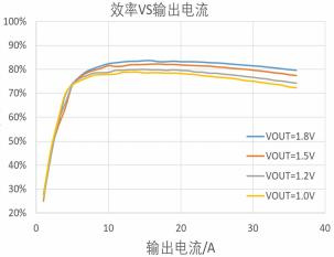
Efficiency | 90 | % | |||
Functionality | Condition | Minimum Value | Nominal Value | Maximum Value | Unit |
VRUN1, VRUN2 thresholds | go up | 1.1 | 1.25 | 1.40 | V |
VRUN1HYS, VRUN2HYS | hysteresis loop |
150 |
mV |
Output Characteristics | Condition | Minimum Value | Nominal Value | Maximum Value | Unit |
Output voltage | 0.6 | 1.8 | V | ||
Linear Regulation | VOUT = 1.5V, VIN from 5V to 15V IOUT = 0A (each) | 0.01 | 0.025 | %/V | |
Load Regulation | VIN = 12V, VOUT = 1.5V, 0A to 18A | 0.75 | 1 | % | |
Output Ripple (per channel) | IOUT = 18A, COUT = 100µF ×3/X7R/Ceramic, 470µF POSCAP, VIN = 12V, VOUT = 1.5V, Frequency = 450kHz | 30 | mV | ||
Dynamic Load Response | 50-100%ILOAD , di/dt=2.5A/μs | 80 | mV | ||
Structural Characteristics | Conditions | Minimum Value | Nominal Value | Maximum Value | Unit |
Size (BGA) | Length | 15.8 | 16 | 16.2 | mm |
Width | 15.8 | 16 | 16.2 | mm | |
Height | 4.91 | 5.01 | 5.21 | mm | |
weights | 2 | g | |||
Environmental Adaptability | Condition | Minimum Value | Nominal Value | Maximum Value | Unit |
Operating temperature (operating junction temperature) | -40 | 125 | ℃ | ||
High temperature storage (ambient temperature) | +125℃ , 48h | 125 | ℃ | ||
High temperature operation (ambient temperature) | +85°C , 24h; Input low, standard and high pressure for 8h each; VIN =12V , VOUT =1.2V , IOUT =10A |
85 | ℃ | ||
Low temperature storage (ambient temperature) | -55°C, 24h | -55 | ℃ | ||
Low temperature operation (ambient temperature) | -40°C , 24h; Input low pressure, standard pressure, high pressure each 8h | -40 | ℃ | ||
Damp heat | High temperature and high humidity stage: 60℃, 95%; Low temperature and high humidity stage: 30℃, 95%; 10 cycles, each cycle is 24h. |
30 |
60 | ℃ | |
Thermal shock | High temperature 125 ℃, low temperature -55 ℃, high and low temperature of an hour for a cycle, a total of 32 cycles of the test | -55 | 125 | ℃ |
NOTE : Stresses above the values listed in the "Limit Values" section may cause permanent damage to the device. Prolonged exposure to any of the absolute maximum ratings may affect the reliability and life of the device
FHT4630 is a dual-output, independently non-isolated DC/DC conversion module. It requires only a few peripheral components to provide two outputs of 18A each. The input voltage range of this module is from 4.5V to 15V, and the output voltage can be adjusted within the range of 0.6V to 1.8V through an external voltage-regulating resistor.
The FHT4630 incorporates a constant-frequency current-mode control regulator and high-speed switching MOSFETs. The typical switching frequency is 500kHz. In applications sensitive to switching noise, the switching frequency can be adjusted within the range of 400kHz to 780kHz through an external synchronization signal. Alternatively, frequency adjustment can be achieved by connecting a resistor from the FSET pin to ground.
Due to its current-mode control and internal loop amplifier, the FHT4630 exhibits excellent loop stability and dynamic performance across a wide range of output capacitance values.
Current-mode control provides cycle-by-cycle current limiting and reverse current limiting. If the output voltage exceeds the ±10% range of the set value, the PGOOD pin will be pulled low. When the output voltage exceeds 10% of the set value, the low-side MOSFET will be turned on to clamp the output voltage, while the high-side MOSFET will be turned off.
Pulling the voltage of the RUN pin below 1.1V will force the corresponding channel into an off state by shutting off the MOSFETs.
The TRACK pin is used to achieve output voltage rise slope control and output voltage tracking, enabling soft-start for the outputs.
The FHT4630 internally integrates a loop compensation network that can adapt to all application conditions. By connecting a resistor from the VFB pin to ground, the output voltage can be adjusted. Additionally, the FHT4630 internally integrates a remote sense differential amplifier, which enables precise detection of the output voltage of one channel or the load point voltage in parallel applications.
Phase shifting can be easily achieved through the MODE_PLLIN, PHASMD, and CLKOUT pins. By programming the PHASMD pin, up to 12 phases of phase shifting can be realized.
By configuring the MODE_PLLIN pin, the skip cycle mode or hiccup mode can be selected to achieve high-efficiency conversion under light loads. This efficient light-load operating mode is ideal for battery-powered applications, effectively extending battery life.
The SW switch pin can be used to monitor whether the operating waveform of the module is normal. Connecting an RC filter circuit to the SW pin can effectively reduce high-frequency ringing at the edges of the high-frequency switching waveform.
Operation
The typical application diagram illustrates the typical application circuit for the FHT4630. The parameters of the peripheral components are mainly determined by the output load current and output voltage.
Input (V_IN) to Output (V_OUT) Step-down Ratio
For a given input voltage, the FHT4630 has a maximum step-down ratio limit. A maximum duty cycle of 98 is possible for each channel, but the minimum voltage difference from input to output is one of the factors limiting the maximum duty cycle of the module. The minimum on-time, tON(MIN) , is another issue to consider. At a certain operating frequency, tON(MIN) < D/fSW , D is the duty cycle and fSW is the switching frequency. The minimum value of tON(MIN) is 90 ns for the electrical parameters.
Output Voltage Setting
The PWM controller of the FHT4630 incorporates a built-in 0.6V reference voltage, and there are 60.4kΩ feedback resistors connected between VOUTS1 and VFB1, as well as between VOUTS2 and VFB2, respectively. Users can adjust the voltage for both output channels independently. If at least one of VOUTS1 and VOUTS2 is floating during independent output or parallel application, an output overvoltage fault will occur. If VFB1 or VFB2 is floating, the output voltage will default to 0.6V. By connecting a resistor between VFB1 or VFB2 and GND, the output voltage can be adjusted
VFB Resistance vs. Output Voltage
For parallel applications, the same regulating resistor is used for voltage setting.
Input Capacitance
FHT4630, when applied, must be connected to a DC source with low AC internal resistance. To achieve input voltage filtering, it is recommended to add four 22μF ceramic capacitors at the input terminals. Additionally, a 47μF to 100μF electrolytic capacitor can be added to increase the input capacitance.
For a BUCK converter with a duty cycle of one switching cycle
It can be estimated as:

Without considering the inductor current ripple, the input capacitor ripple current for each channel can be estimated as:

In the above equation, η % is the estimated efficiency of the power module. Electrolytic capacitors or polymer capacitors can be used as high-capacity main filter capacitors.
Output Capacitance
The FHT4630 has low output voltage ripple and good dynamic performance. Low ESR output capacitors should be selected to minimize output ripple and improve output dynamics; COUT capacitors can be tantalum, low ESR polymer, or ceramic chip capacitors. Typical output capacitance should be between 200 μF and 470 μF per channel. To further minimize output voltage ripple or improve dynamic performance, the designer can add additional filtering circuitry as needed.
Pulse Burst Mode
Both channels of the FHT4630 can operate in burst mode, where the internal MOSFETs of the module work intermittently, significantly reducing the module's power consumption under light loads. In applications where high efficiency under light loads is required, burst mode can be employed. To activate burst mode, the MODE_PLLIN pin should be left floating.
Furthermore, the module employs an internal current-mode control strategy, which enables excellent current-sharing performance in parallel configurations, thereby achieving good thermal balancing among the modules.
Frequency selection and phase-locked loops
The FHT4630 can achieve higher conversion efficiency by adjusting its switching frequency. The switching frequency can be adjusted by varying the resistance between the fSET pin and SGND (ground). The fSET pin outputs a precise 10μA current source, and the voltage generated by this current flowing through the resistor to ground allows for the adjustment of the operating frequency. Alternatively, an external voltage can be applied to the fSET pin to program the operating frequency.
The diagram above illustrates the relationship between the voltage at the FSET pin and the operating frequency. Additionally, the FHT4630 allows for synchronization of
its switching frequency and phase with an external signal by inputting a CLOCK signal (ranging from 400kHz to 780kHz) through the MODE_PLLIN pin.
The high-level threshold for the input CLOCK signal is 1.6V, and the low-level threshold is 1V.
Pulse Skipped Modulation
In applications where achieving low output ripple and
high efficiency under half-load conditions is desired,
the pulse skipped cycle mode (or pulse skip modulation, PSM) can be adopted. In this mode, the module is allowed to enter the skipped cycle state under light loads, which reduces switching losses and thereby enhances efficiency under such conditions. By pulling the MODE_PLLIN pin up to INTVcc, the module can be enabled to operate in the pulse skipped cycle mode.
Forced Continuous Conduction Mode
In applications where a fixed operating frequency is preferred over high efficiency at low loads, and where lower output ripple is simultaneously desired, the forced continuous mode (FCM) can be employed. By pulling the MODE_PLLIN pin down to GND, the module can be set to operate in the forced continuous mode. In this mode, the internal inductor current is allowed to flow in reverse under no-load or light-load conditions, and the internal upper switch will be turned on in every switching cycle. However, during the startup process of the module, the forced continuous mode is disabled, and the inductor current is prevented from flowing in reverse until the output voltage rises to its normal level, at which point the forced continuous mode is engaged.
Multi-phase parallel mode
When the required output current exceeds 18A, two FHT4630 modules can be connected in parallel. For even higher output currents, multiple FHT4630 modules can be paralleled. Paralleling does not increase input current ripple or output voltage ripple. The FHT4630 can also be synchronized to an external clock signal (between 400kHz and 780kHz) via the MODE_PLLIN pin, and the internal phase-locked loop locks this external input signal to the internal phase. Additionally, the CLKOUT signal can be connected to the MODE_PLLIN pin of the next module to achieve frequency synchronization and phase interleaving. By configuring the PHASMD pin to INTVCC, SGND, or leaving it open, a phase shift of 120°, 60°, or 90° (between MODE_PLLIN and CLKOUT) can be achieved. By configuring the PHASMD pins of the paralleled modules differently, up to 12-phase interleaved paralleling can be realized.
The use of multi-phase interleaved paralleling with FHT4630 can effectively reduce current ripple on both the power input and output sides.
Output Voltage Tracking
The TRACK pin is used for output voltage tracking control by connecting a capacitor to ground. The TRACK pin outputs a constant current of 1.3μA, which charges the external capacitor. The voltage on the external capacitor rises until it reaches the level of INTVcc. Before reaching an internal reference voltage of 0.6V, the output voltage is controlled by the voltage on the TRACK pin. Once the reference voltage is reached, the output voltage is no longer controlled by the TRACK pin voltage but instead by the difference between the internal reference voltage and the feedback voltage, which is processed to control the output voltage. During this startup sequence or soft-start process, the current feedback control is disabled. When the voltage on the enable pin (RUN) is below 1.2V, the TRACK pin is forcibly pulled low. The entire soft-start time can be calculated using the following formula:.

Operation
Power Good
Inside the module, the Power Good (PGOOD) pin is configured as an open-drain output under normal conditions. This pin can be used to detect whether the output voltage is within ±10% of its normal regulated value. By connecting an external pull-up resistor to a specific voltage (not exceeding 6V), you can monitor the output voltage.
Loop Compensation
A loop stabilization compensation system for all output voltages is already integrated within the FHT4630, eliminating the need for external design.
Enabling Control
The enable pin of the FHT4630 has a typical turn-on voltage threshold of 1.25V, with a maximum threshold of 1.4V, and incorporates a 150mV hysteresis function. The enable pin controls the activation of the corresponding channel and INTVcc.
When the input voltage is 5V, the RUN pin can be directly pulled up to VIN. When the input voltage exceeds 5V, the RUN pin should be pulled up to VIN through a resistor ranging from 10kΩ to 100kΩ, and a 5V zener diode should be connected between this pin and ground. In multi-phase parallel applications, the RUN pins can be tied together to be controlled uniformly by a single signal.
INTVCC and EXTVCC
The FHT4630 is equipped with an internal linear regulator that converts the input voltage to a 5V output, which powers the internal control circuitry and MOSFET drivers of the module. This 5V output voltage is controlled by either RUN1 or RUN2.
Additionally, the FHT4630 allows for an external 5V control voltage to be supplied to the module through the EXTVcc pin, which can reduce power loss and improve efficiency. The minimum valid input voltage for the EXTVcc pin is 4.7V, with a maximum of 6V. When providing control voltage through the EXTVcc pin, it must be applied after VIN and prior to VIN being turned off..
Remote Differential Sampling Amplifier
The FHT4630 provides a precision remote differential sampling amplifier that accurately samples lower output voltages at remote load points. This remote sampling is particularly suitable for high-current load applications. The remote differential sampling amplifier can be used for either channel 1 or channel 2, or for output voltage sampling in parallel applications.
It is important to note that DIFFP and DIFFN should be connected to the corresponding positions for output voltage sampling, while DIFFOUT should be connected to either VOUTS1 or VOUTS2. In parallel applications, DIFFP and DIFFN should be connected to the corresponding positions for the output voltage, and DIFFOUT should be connected to either VOUTS1 or VOUTS2, depending on the specific configuration.
SW pin
The SW pin primarily serves for testing and monitoring purposes. Additionally, it can be used to suppress ringing generated by parasitic LC parameters in the current loop. Typically, an RC series absorption circuit is connected to this pin and grounded to absorb ringing interference. By selecting an appropriate capacitance value, only high-frequency interference is allowed to pass through the resistor and be absorbed.
PCB Layout
The FHT4630 module has highly integrated most of the functions of DC-DC conversion, making the user's PCB design relatively simple. However, in PCB design, it is still necessary to optimize the layout and routing as much as possible to achieve optimal electrical and thermal performance.
• The VIN, GND, VOUT1, and VOUT2 should incorporate large-area copper pouring to minimize parasitic impedance and thermal resistance.
• Place high-frequency ceramic capacitors in close proximity to VIN-to-GND and VOUT-to-GND connections to minimize switching noise.
• Designate a dedicated ground layer on the underside of the module.
• To mitigate losses incurred by vias under high-current conditions and to decrease thermal resistance, employ multiple vias in parallel, connecting the large-area copper pouring on the PCB's top layer to other layers.
• Utilize a separate copper pouring design within the signal ground (SGND) area and connect it to GND at a single point on the module's bottom side.
• In parallel applications, ensure that the VFB, VOUT, and COMP pins of each channel are connected as closely together as feasible.
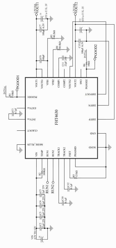
Typical Circuit Two Phase Independent Output Application Example
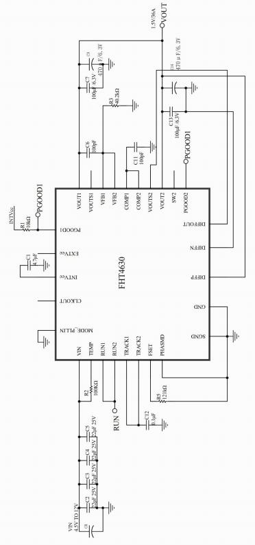
Typical Circuit Two Phase Parallel Output Application Example
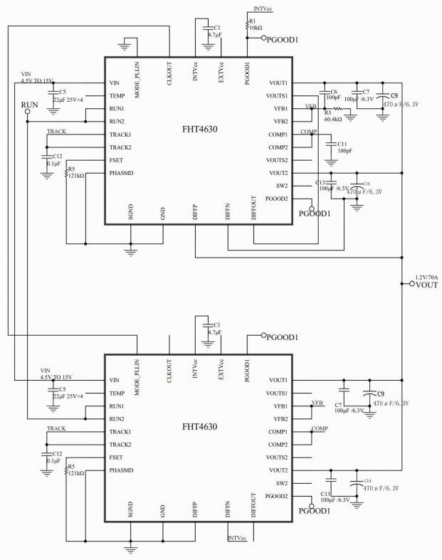
Typical Circuit 4-Phase Parallel Output Application Example
Package Description
LGA (16mm x 16mm x 4.32mm)
BGA (16mm x 16mm x 5.01mm)
Soldering and Storage Precautions
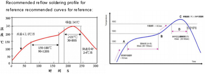
For lead-free BGA solder ball products, the peak temperature should not exceed 245°C. For lead-based BGA solder ball products, the peak temperature should not exceed 225°C.
Caution:
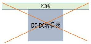
1.Due to the large size of the module, please do not place the module under the board for reflow soldering to avoid falling off.
2.For bulk products and those that have been taken out of their original packaging, they should be stored in a desiccator (with a relative humidity of less than 10% inside). For products still in their original packaging, they should also be stored in a desiccator whenever possible.
3.Before mounting on the board, it is necessary to strictly follow the baking conditions to dry the samples: bake at 125°C for more than 48 hours, and control the reflow soldering temperature within 245°C.
Product Model | Input | Output | Packaging | Grade | Temperature Range (Case Temperature) | Packaging |
FHT4630IY | 4.5~15V | 0.6~1.8V | BGA (leaded) | Industrial grade | -40-125°C | Tray |
FHT4630IY#PBF | 4.5~15V | 0.6~1.8V | BGA (lead-free) | Industrial grade | -40-125°C | Tray |
FHT4630IV#PBF | 4.5~15V | 0.6~1.8V | LGA (lead-free) | Industrial grade | -40-125°C | Tray |
FHT4630MY | 4.5~15V | 0.6~1.8V | BGA (leaded) | General military grade | -55-125°C | Tray |
FHT4630MY#PBF | 4.5~15V | 0.6~1.8V | BGA (lead-free) | General military grade | -55-125°C | Tray |
FHT4630MV#PBF | 4.5~15V | 0.6~1.8V | LGA (lead-free) | General military grade | -55-125°C | Tray |
| Item | Description | Reel/Tray | Pcs/Roll | G.W | N.W | QTY/Carton | Package Size |
FHT4630 | Input 4.5V-15V, output 0.6V-1.8V Dual-Channel DC/DC Adjustable Buck Converter Module SIP Packaged Efficiency up to 94% |
| 500pcs | kgs | kgs | 500pcs | 210*210*50mm |
Discover all the technical specifications by downloading the datasheet today.
| Part Number |
Output Current
(A) |
Input Voltage
(V) |
Output Voltage
(V) |
Dimensions(mm) |
Maximum
Efficienc |
Factory Pack
Quantity |
Footprint 3D | Datasheet | Sample |
| UDM2520I | 0.6A | 2.3V ~ 5.5V | 0.8V~3.3V | 2.5mm × 2mm x 1.1mm | 94% | 3,000pcs |  |
 |
|
| UDM22006 | 0.6A | 2.3V~5.5V | 1.2V~3.3V | 2.5mm x 2mm x 1.1mm | 95% | 3,000pcs | |
|
|
| UDM22010 | 1A | 2.3V ~ 5.5V | 1.2V ~ 3.3V | 2.5mm x 2mm x 1.1mm | 95% | 3,000pcs | |
|
|
| UDM82821adj | 1A | 2.5V~5.5V | 0.8V~4V | 2.5mm × 2mm x 1.1mm | 95% | 3,000pcs | |
|
|
| UDM82821 | 1.2A | 2.3V~5.5V | 1.2V~3.3V | 2.5mm × 2mm x 1.1mm | 95% | 3,000pcs | |
|
|
| UDM2826I | 1.5A | 2.7V ~ 5.5V | 1V ~ 3.3V | 2.8mm × 2.6mm x 1.1mm | 93% | 3,000pcs | |
|
|
| UDM3606 | 0.6A | 4.5V-18V | 0.6V-5.5V | 5mm×3.2mm×2.2mm | 95% | 3,000pcs | |
|
|
| UDM3506 | 0.6A | 4.7V-36V | 0.8V | 5mm×3.2mm×2.2mm | 88% | 3,000pcs | |
|
|
| UDM3610 | 1.2A | 4.5V~18V | 0.6V~5.5V | 5mm×3.2mm×2.2mm | 95% | 3,000pcs | |
|
|
| UDM92403 | 0.3A | 0.7V~5.5V | 1.8V~5.5V | 2.5mm×2mm x 1.1mm | 93% | 3,000pcs | |
|
|
| UDM81256 | 1A | 2.5V ~ 5.5V | 5V | 2.8mm×2.6mm×1.35mm(1.1mm) | 95% | 3,000pcs | |
|
|
| FHT4644 | 4A | 4.0V ~ 15V | 0.8V ~ 5.5V | 9mm x 15mm x 4.32mm | 92% | 500pcs | |
|
|
| FHT4644H | 4A | 4.0V ~14V | 0.6V ~ 5.5V | 9mmx15mmx4.32mm | 92% | 500pcs | |
|
|
| FHT4644C/D | 4A | 4.5V-14V | 0.6V-5.5V | 9mmx15mmx4.32mm | 92% | 500pcs | |
|
|
| FHT4644F | 4A | 4.5V ~ 16V | 0.6V ~ 5.5V | 9.0mmx15mmx4.32mm | 92% | 500pcs | |
|
|
| FHT4644L | 4A | 4.0V ~15V | 0.8V ~ 5.5V | 9mmx15mmx1.82mm | 92% | 500pcs | |
|
|
| FHT4630 | 18A+18A | 4.5V~15V | 0.6V ~ 1.8V | 16mm × 16mm × 5.01mm | 94% | 500pcs | |
|
|
| FHT3860 | 6A | 2.3V-5.5V | 0.5V-3.3V | 4mm x 6mm x 1.6mm | 94% | 500pcs | |
|
|
| FHM3695-25 | 20A | 4V-16V | 0.6V-5.5V | 10mm × 12mm ×4.32mm | 95% | 500pcs | |
|
|
| FHT4623 | 3A | 4.2V-20V | 0.6V-5.5V | 6.75mm x 6.75mm x 2.95mm | 95% | 500pcs | |
|
|
| MPPM8070 | 2A | 4.5V-18V | 0.6V-15V | 8mm×7mm × 4.32(2.5mm) | 93% | 500pcs | |
|
|
| FHT4618 | 6A | 4.5V-24V | 0.6V-5.5V | 15mm×9mm×4.32mm | 95% | 500pcs | |
|
|
| FHT23030 | 3A | 4.5V-17V | 0.9V-6V | 3mm×2.8mm×1.4mm | 94% | 500pcs | |
|
|
| FHT3550 | 5A | 3.5V-40V | 1.0V-12.0V | 12mm x 12mm x 4.32mm | 95% | 500pcs | |
|
|
| FHT8027C | 4A | 5V-60V | 2.5V-24V | 15mm×15mm×4.32mm | 95% | 500pcs | |
|

Data Centers and Server Farms

Medical Devices

Aerospace and Defense

Automotive Electronics

Industrial and Automation

Consumer Electronics

Telecommunications and Networking