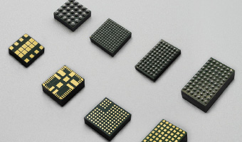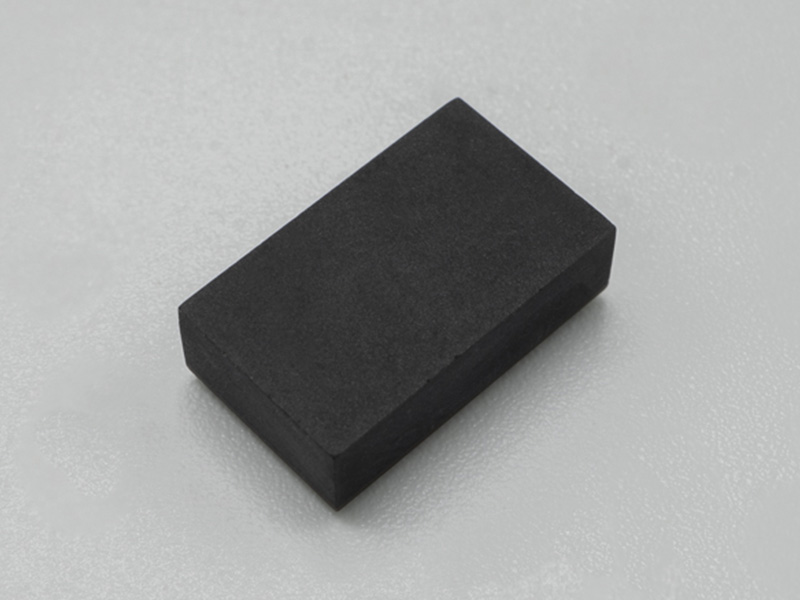


 Integrated Magnetic Power Module
Buck (Step-Down)-Low Voltage
Buck (Step-Down)-Medium Voltage
Boost (Step-Up)
DC-DC Power Modules
Integrated Magnetic Power Module
Buck (Step-Down)-Low Voltage
Buck (Step-Down)-Medium Voltage
Boost (Step-Up)
DC-DC Power Modules
 Magnetically Integrated Power Module (SiP)
Buck (Step-Down)-Multiple Outputs
Buck (Step-Down)
Boost (Step-Up)
Magnetically Integrated Power Module (SiP)
Buck (Step-Down)-Multiple Outputs
Buck (Step-Down)
Boost (Step-Up)
 Customized DC-DC Converters
Tailored Power Modules: Precision Solutions for Your Unique Needs.
Contact Us Today to Discuss Your Project!
DC-DC Power Modules
Customized DC-DC Converters Explore DC-DC Converters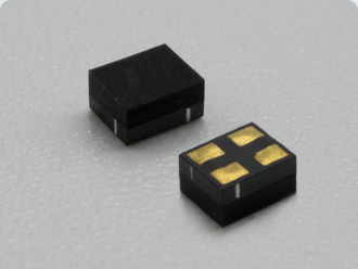
UDM22006 DC DC Integrated Magnetic Power Module ( Input 2.3V–5.5V, output 1.2V-3.3V )
Details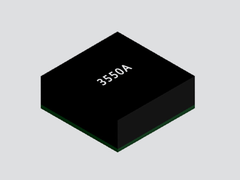
FHT3550 DC/DC Adjustable Buck Power Module ( 3.5V-40V Input, 1.0V-12.0V Output )
Details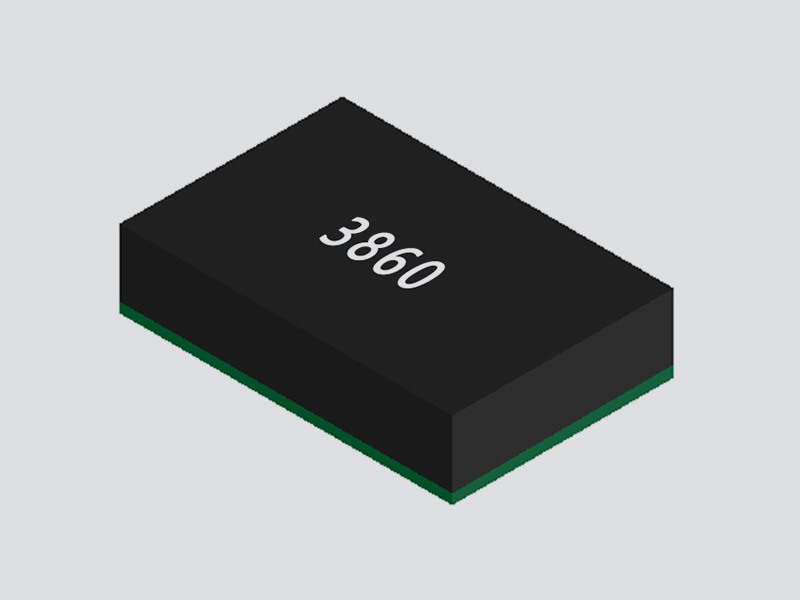
FHT3860 DC/DC Step-Down Buck Power Module ( 2.3V-5.5V Input, 0.5V-3.3V Output )
Details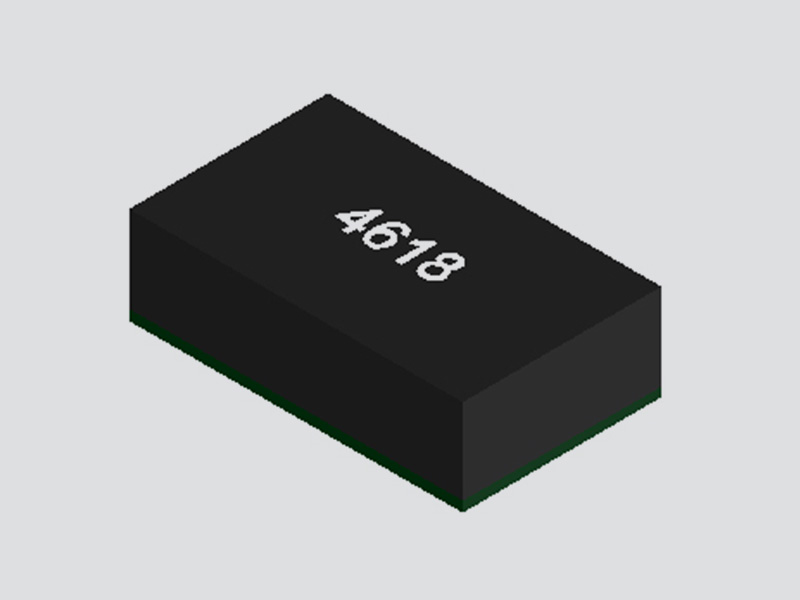
FHT4618 Integrated DC/DC Adjustable Buck Power Module ( 4.5V-24V Input, 0.6V-5.5V Output )
Details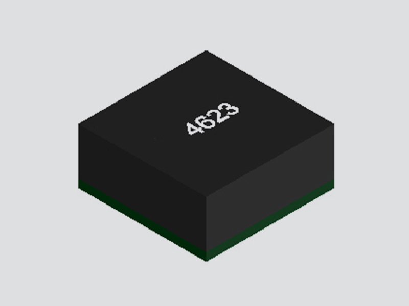
FHT4623 DC/DC Adjustable Buck Converter Power Module ( 4.2V-20V Input, 0.6V-5.5V Output )
Details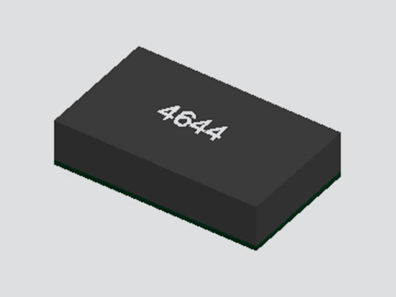
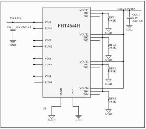
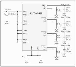
FHT4644 Ultra-Thin Multi-Channel DC/DC Buck Power Module ( 4.0V ~ 15V Input, 0.8V ~ 5.5V Output )
Details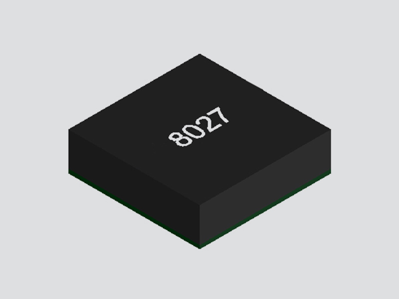
FHT8027C DC/DC Buck Converter Integrated Power Module ( 5V-60V Input, 2.5V-24V Output )
Details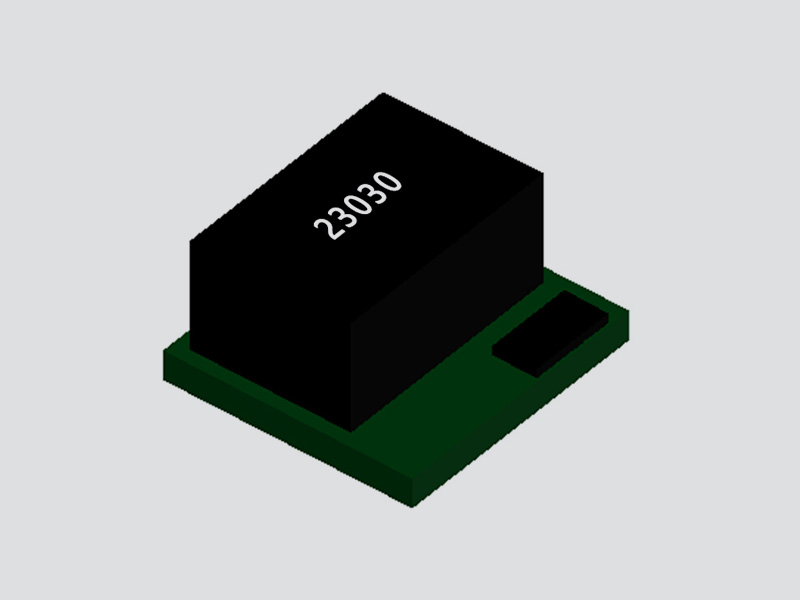
FHT23030 DC/DC Adjustable Buck Converter Module ( 4.5V–17V Input, 0.9V–6V Output )
Details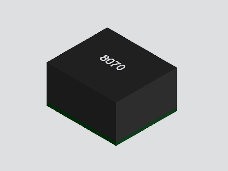
MPPM8070 DC/DC Adjustable Buck Converter Module ( Input 4.5V–18V, Output 0.6V-15V )
Details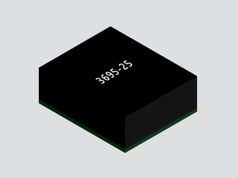
FHM3695 DC/DC Adjustable Buck Power Module ( 4V-16V Input, 0.6V-5.5V Output )
Details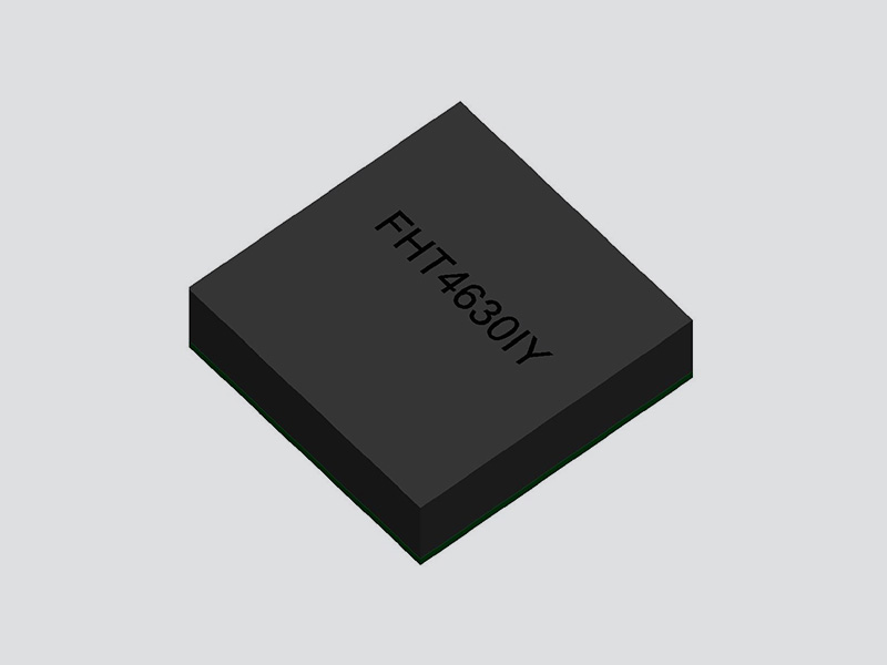
FHT4630 Dual-Channel DC/DC Adjustable Buck Converter Module ( 4.5V~15V Input, 0.6V ~ 1.8V Output )
Details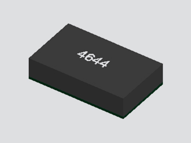
FHT4644C/D 4-Channel DC/DC Buck Power Module with Adjustable Outputs ( 4.5V-14V Input, 0.6V-5.5V Output )
Details
FHT4644F 4-Channel DC/DC Magnetically Integrated Buck Power Module (SiP) | 4.5V to 16V Input, 0.6V to 5.5V Output
Details
FHT4644L 4-Channel Integrated Adjustable Buck DC/DC Power Module ( 4.0V ~ 15V Input, 0.8V ~ 5.5V Output )
Details
UDM2520I Integrated DC/DC Buck Step-Down Power Module ( 2.3V-5.5V Input, 0.8V-3.3V Output )
Details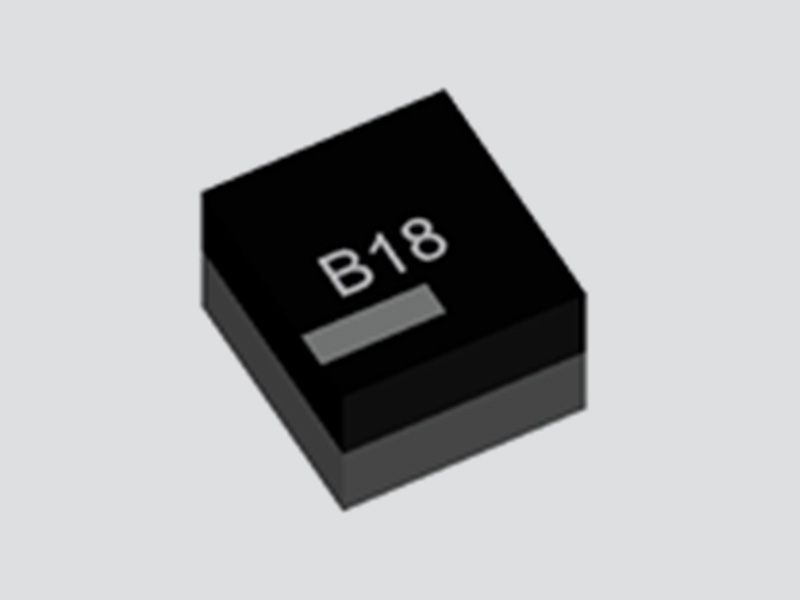
UDM2826I Integrated DC-DC Buck Step-Down Power Module ( 2.7V-5.5V Input, 1.0V-3.3V Output )
Details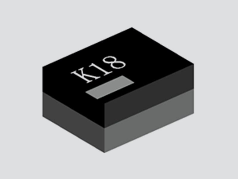
UDM22010 Integrated DC-DC Buck Step-Down Power Module ( 2.3V-5.5V Input, 1.2V-3.3V Output )
Details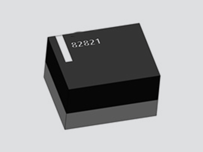
UDM82821 Integrated Magnetic DC-DC Buck Step-Down Power Module ( 2.3V-5.5V Input, 1.2V-3.3V Output )
Details
UDM82821adj Magnetically Integrated DC-DC Buck Power Module ( 2.5V-5.5V Input, 0.8V~4.0V Output )
Details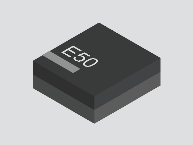
UDM81256 Integrated DC-DC Boost Power Module ( 2.5V-5.5V Input, Fixed 5V Output )
Details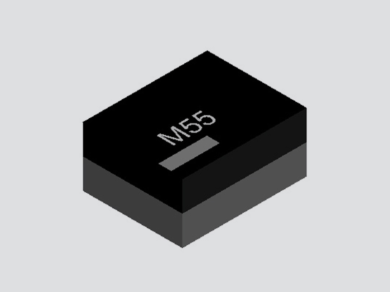
UDM92403 Integrated DC-DC Boost Step-Up Power Module ( 0.7V-5.5V Input, Adjustable 1.8V-5.5V Output )
Details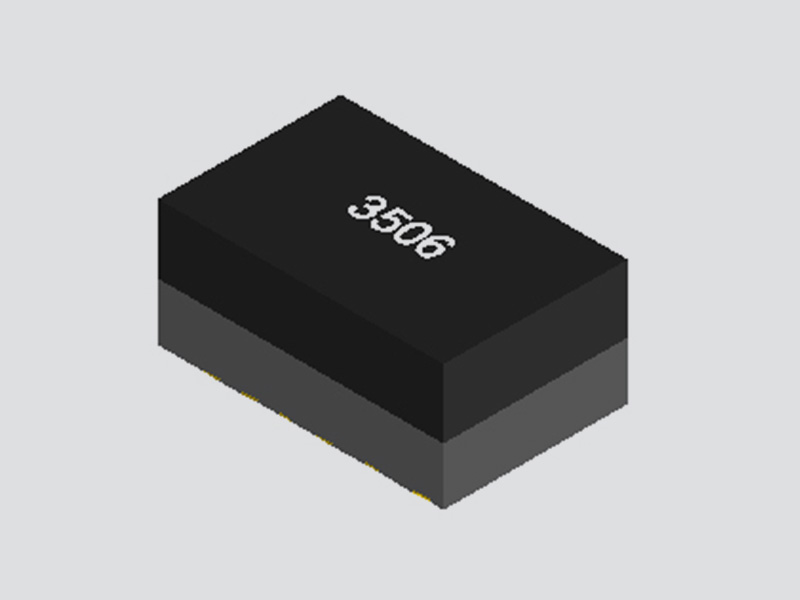
UDM3506 Integrated DC-DC Buck Step-Down Power Converter Module ( 4.7V-36V Input, 0.8V Output )
Details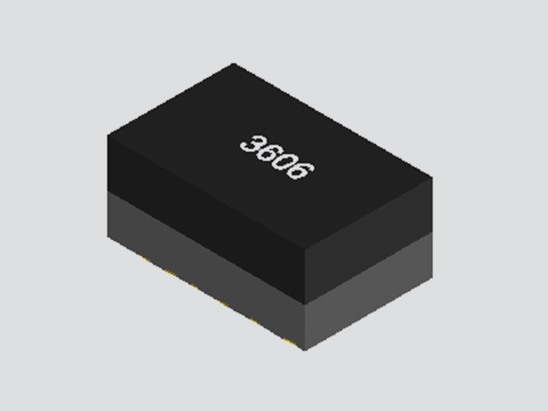
UDM3606 Integrated Medium Voltage DC-DC Buck Step-Down Power Module ( 4.5V-18V Input, 0.6V-5.5V Output )
Details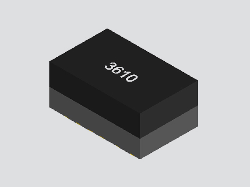
UDM3610 Integrated Medium Voltage DC-DC Buck Step-Down Power Supply Module ( 4.5V-18V Input, 0.6V-5.5V output )
Details4A continuous full load output current per circuit
Wide input voltage range: 4.0V to 14V
Output voltage range: 0.6V to 5.5V
Switching frequency: Typical 1 MHZ
High efficiency: 92%
Internal 1mS soft start (additional external 1mS optional)
±1.5% total output voltage regulation
Over-current protection, over-temperature protection, over-voltage protection, under-voltage protection
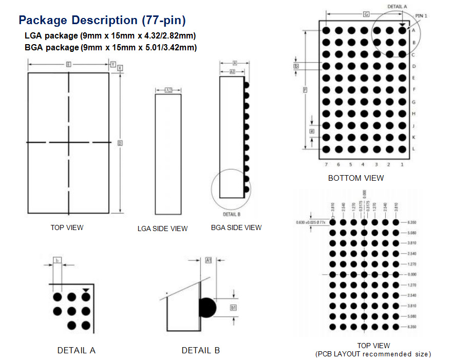
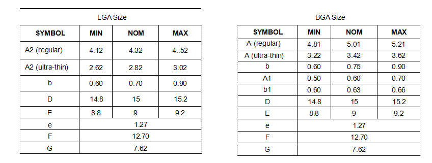
Regular size:
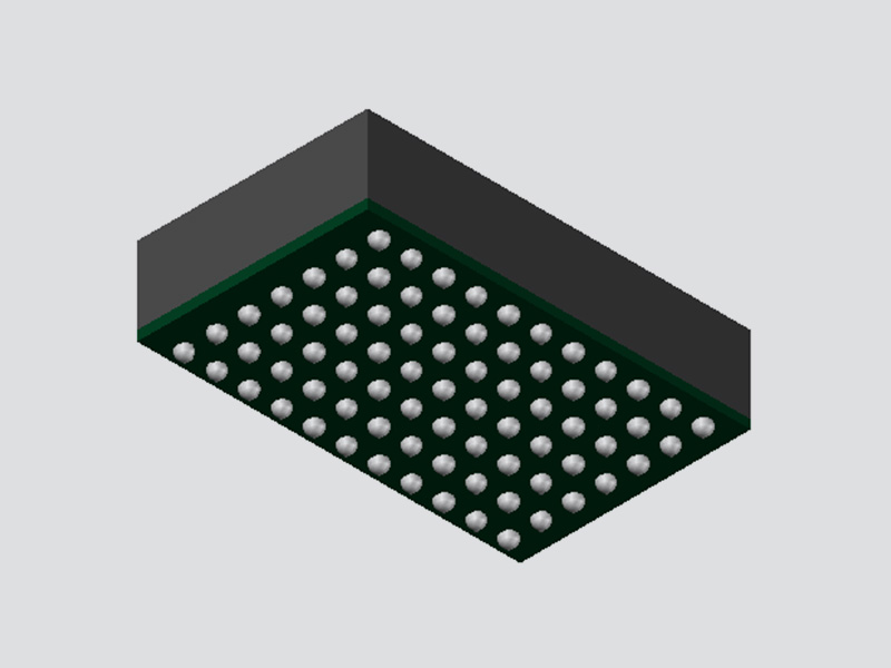
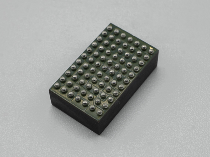
LGA package (9mm*15mm*4.32mm)
BGA package (9mm*15mm*5.01mm)
Ultra-thin size: less than half the thickness of regular size
LGA package(9mm*15mm*2.82mm)
BGA package(9mm*15mm*3.42mm)
Multi-rail point-of-load regulation; CPU and GPU power supply
Power supply for ASIC chips
The FHT4644H is a non-isolated step-down all-in-one molded point power supply for embedded high-current load points. Its size is only 9 x 15 x 2.42mm and can be placed directly next to the FPGA/CPU, making it ideal for low output voltage, multi-application applications.
The small size of the LGA and BGA package integrated IC, inductors and the corresponding components, only need to configure a peripheral voltage regulator resistor, a few input and output ceramic capacitors, you can quickly complete the design of the multi-channel power supply system to simplify the design of the system, maximize the savings of PCB space.
Based on synchronous rectification Buck topology, maximum 4A per circuit, high power conversion efficiency, can be converted from 4.0V to 14V.
0.6~5.5V, provide four-way ON/OFF control, four-way Power Good, OCP (over-current), OVP (over-voltage), UVP (under-voltage), OTP (over-temperature), SCP (short-circuit) protection.
Configurable output array
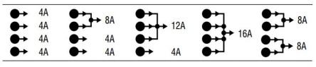
Quad Output Application Circuit
Non-parallel applications Parallel
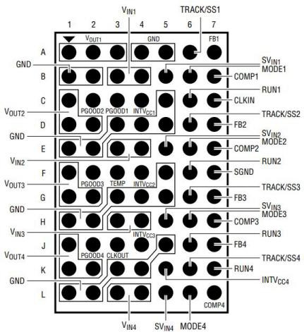
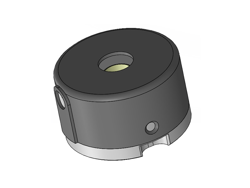
77-Pins (16mm x 9mm x 5.01mm)
Pin | Description |
VOUT1 (A1,A2,A3), VOUT2 (C1,D1,D2), VOUT3 (F1,G1,G2), VOUT4 (J1,K1,K2), | Power Module Quad Output Pins |
VIN1 (B3,B4),VIN2 (E3,E4),VIN3 (H3,H4),VIN4 (L3,L4) | Power Module Quad Input Pins |
GND (A4,A5, B1,B2, C5, D3,D4,D5, E1,E2, F5, G3,G4,G5,) h1, h2, j5, k3, k4, l1, l2) | Ground pin |
fb1 (a7), fb2 (d7), fb3 (g7), fb4 (j7) | The four output voltage adjustment pins can be connected to GND with 0.5% accuracy voltage adjustment resistors. |
run1 (c6), run2 (f6), run3 (j6), run4 (k7) | The four enable pins can be directly connected to the input voltage, or connected to an external power supply to control the power module. The minimum enable voltage is 1.1V, and when the enable voltage is lower than 0.95V, the power supply will be turned off. It is recommended that the enable voltage is greater than 1.2V, this pin can not be suspended. |
pgood1 (c3), pgood2 (c2), pgood3 (f2), pgood4 (j2) | Fault indication pin, PG = high means VOUT is within the voltage range, PG = low means VOUT is below the specified value. This PGOOD pin can be connected to a 100K resistor to the INTVCC pin, or other voltages can be supplied to the INTVCC pin. PGOOD , when PGOOD is low, it indicates an abnormality in the power module (the said abnormality includes) (UV, OV, OC, OT, etc.), if the fault indication function is not required, this resistor may not be added, and PGOOD can be left vacant. |
INTVCC1 (C4), INTVCC2 (F4), INTVCC3 (J4), INTVCC4 (K5) | Internal power drivers and control circuits are powered from these pins, each of which is internally decoupled to GND using a 1μF low ESR ceramic capacitor. |
MODE1(B6), MODE2(E6), MODE3(H6), MODE4(L6) | Operating Mode pin , different operating modes can be selected for each channel. Provides forced CCM under light load conditions (The MODE pin is used to switch the resistor RM between SGND or INTVCC to enable 2 different switching frequencies and 2 light load modes. Two different switching frequencies and two light load modes can be realized by switching resistor RM between SGND or INTVCC via the MODE pin, which cannot be left idle. |
SGND (F7) | For signal ground, it is recommended that GND (power ground) and SGND be wired separately and eventually connected with a 0 ohm resistor. |
TRACK/SS1 (A6), TRACKSS2 (D6), TRACK/SS3 (G6), TRACKSS4 (K6) | External soft start pin, external 33 to 100nF ceramic capacitor can be connected to the signal ground, if you do not need to add external soft start function, do not add this capacitor, SS pin is left empty. |
SVIN1 (B5), SVIN2 (E5), SVIN3 (H5), SVIN4 (L5) | The internal power supply pin, which provides the input voltage source for the internal 3.3V regulator, is normally connected to the VIN pin. The external power supply connected to SVIN must be at least 4V and must also be greater than VOUT. |
COMP1(B7),COMP2(E7),COMP3(H7),COMP4(L7) | Internal compensation pin to stabilize the loop. When modules are used in parallel, the COMP pins need to be connected together. |
CLKIN (C7) | External synchronization input to the module's phase detector. This pin has been terminated internally with a 20kΩ resistor to SGND. The phase-locked loop will force the channel 1 lead signal to synchronize with the rising edge of the CLKIN signal. Channels 2, 3 and 4 will also be synchronized to the rising edge of the CLKIN signal with a predetermined phase shift. |
CLKOUT (J3) | The output clock signal of the module. the phase of CLKOUT is set to 180° with respect to CLKIN. |
TEMP (F3) | An on-board temperature monitoring diode used to monitor the change in junction voltage with temperature. See Application Information section. |
Absolute Maximum Ratings | Condition | Minimum value | Nominal value | Maximum value | Unit |
VIN (each way) | -0.3 | 22 | V | ||
VOUT (each way) | -0.3 | 6 | V | ||
INTVCC. CLKOUT,CLKIN | -0.3 | 3.6 | V | ||
FB, PGOOD (each way) | -0.3 | 3.6 | V | ||
PGOOD current (per circuit) | 10 | mA | |||
MODE, SS/TR (each way) | -0.3 | 3.6 | V | ||
RUN (each way) | -0.3 | 22 | V | ||
storage temperature | -55 | 150 | ℃ | ||
Reflow temperature | 245 | ℃ | |||
Input Characteristics | Condition | Minimum value | Nominal value | Maximum value | Unit |
Input Voltage Range | 4.0 | 12 | 14 | V | |
Power-on voltage threshold | 3.5 | V | |||
Shutdown Voltage Threshold | 2.4 | 2.6 | 2.8 | ||
Input current at full load | VIN =12V , VOUT =1.5V , IOUT =4A | 0.6 | A | ||
Input current at low voltage full load | VIN =5V , VOUT =1.5V , IOUT =4A | 1.5 | A | ||
Input current at no load | VIN =12V , VOUT =1.5V , IOUT =0A | 650 | μA | ||
Static Input Current | ON/OFF =OFF | 15 | μA | ||
General Requirements | Condition | Minimum Value | Nominal Value | Maximum Value | Unit |
Switching Frequency | Automatic Adjustment | 1000 | KHz | ||
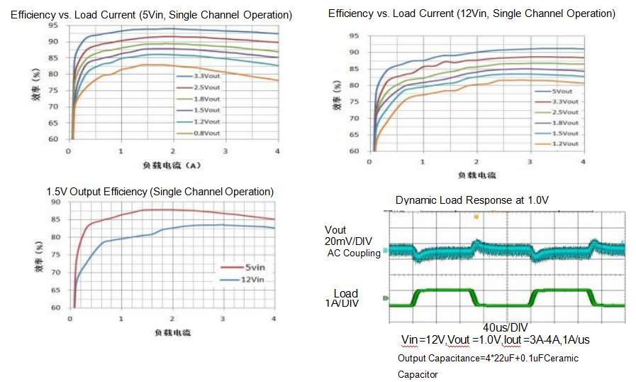
Efficiency | Vin=5V , Vout=3.3V | 92 | % | ||
Soft Start Time | SS pin with 3.3nF ceramic capacitor | 2 | ms | ||
Enable | Condition | Minimum value | Nominal value | Maximum value | Unit |
RUN enable voltage | 1.2 | - | 14 | V | |
Output Characteristics | Condition | Minimum value | Nominal value | Maximum value | Unit |
Output Voltage Range | Adjusted by FB pin resistor | 0.6 | 5.5 | V | |
Output Voltage | CIN = 22µF, COUT = 22uF×4, VIN = 4V to 14V, IOUT = 0A to 4A |
1.47 |
1.5 |
1.53 | V |
Linear Regulation | VOUT = 1.5V , 4V < VIN < 14V , ILOAD = 4A | ±0.05 | % | ||
Load Regulation | VIN =12V , VOUT =1.5V,1A < ILOAD ≤ 4A | ±1 | % | ||
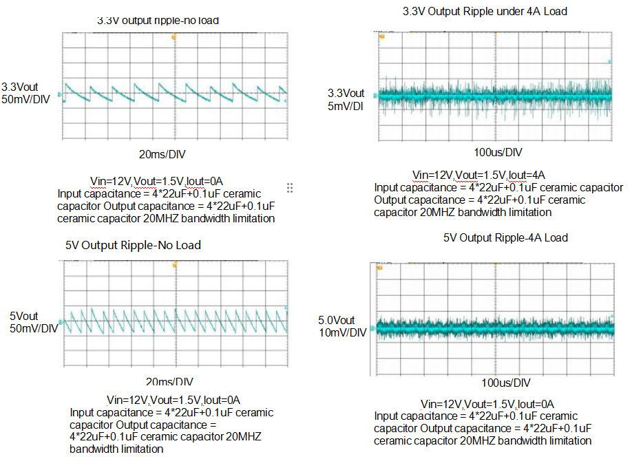
Ripple and Noise | VIN =12V , VOUT =1.5V , IOUT =4A, Cout =22uF×4 , 20MHz bandwidth |
10 |
50 |
mV | |
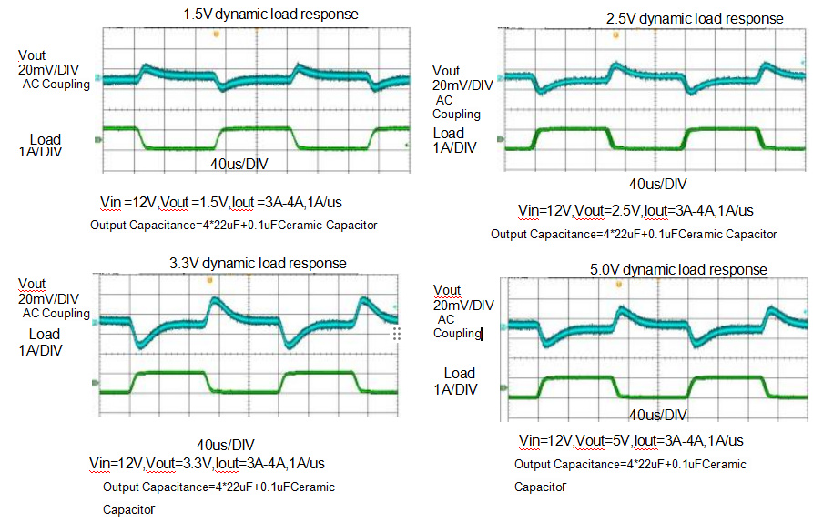
Dynamic Load Response | 75-100% full load , di/dt = 1A/μS Cout =22uF×4 | 50, 40 | mV , µs |
Output Characteristics | Condition | Minimum value | Nominal value | Maximum value | Unit |
Output Overcurrent Protection | Iout% | 115 | 120 | 125 | % |
Output Overvoltage Protection | Vout% | 115 | 115 | 130 | % |
Over-Temperature Protection | Case temperature (Tc) | - | - | 135 | ℃ |
Structural Characteristics | Conditions | Minimum Value | Nominal value | Maximum value | Unit |
Packaging | LGA, BGA | - | - | - | - |
Size | lga: 9*15*4.32; bga: 9*15*5.01 | - | - | - | mm |
Weights | 1.6 | g | |||
Environmental Adaptability | Condition | Minimum value | Nominal value | Maximum value | Unit |
Operating temperature (Case temperature) | -55 | 125 | ℃ | ||
High temperature storage (ambient temperature) | +125℃ , 48h | 125 | ℃ | ||
High temperature operation (ambient temperature) | +85°C , 24h; Input low voltage, standard voltage, load derating, high voltage each 8h | 85 | ℃ | ||
Low temperature storage (ambient temperature) | -55°C, 24h | -55 | ℃ | ||
Low temperature operation (ambient temperature) | -55°C , 24h; Input low pressure, standard pressure, high pressure each 8h | -55 | ℃ | ||
Damp heat | High temperature and high humidity stage: 60°C, 95%; Low temperature and high humidity stage: 30℃, 95%; 10 cycles, each cycle is 24h. | 30 | 60 | ℃ | |
Thermal shock | High temperature 125 ℃, low temperature -55 ℃, high and low temperature of an hour for a cycle, a total of 32 test cycles | -55 | 125 | ℃ |
NOTE : Stresses above the values listed in the "Limit Values" section may cause permanent damage to the device. Prolonged exposure to any of the absolute maximum ratings may affect the reliability and life of the device.

The FHT4644H is a quad independent output non-isolated DC/DC switching regulator. It has four independent regulator channels, each capable of delivering up to 4A of continuous output current with minimal external input and output capacitance. Each regulator channel provides a precisely regulated output voltage over the 4.0V to 14V input voltage range of 0.6V to 5.5V through an external resistor.
RUN Start
Pulling the RUN pin of each regulator channel to ground forces the regulator into a shutdown state, turning off the power MOSFETs and most of the internal control circuitry. Placing the RUN pin above 0.7V only turns on the internal reference while still keeping the power MOSFETs off. Further increasing the RUN pin voltage above 1.2V will open the entire regulator channel.
Output Voltage Setting
Inside the FHT4644H, the FB pin is connected to the VOUT terminal of each channel through a 60.4kΩ precision resistor. The output voltage of this module can be controlled by programming the resistance between the FB and GND pins. The calculation is as follows: Please refer to the formula below for the calculation:
Note: It is recommended to reserve two resistor positions with a precision of 0.5% for fine-tuning of the output voltage. The following formula is used for calculating the output voltage adjustment resistor:
Vout (V) | 0.6 | 1.0 | 1.2 | 1.5 | 1.8 | 2.5 | 3.3 | 5.0 |
RFB (kΩ) | open | 90.9 | 60.4 | 40.2 | 30.1 | 19.1 | 13.3 | 8.25 |
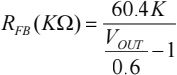
Table 1 below shows the relationship between the RFB resistance and each output voltage.
Table 1 RFB resistor versus each output voltage
Switching Frequency Selection
The operating frequency of the FHT4644H has been optimized to achieve a compact package size and minimal output ripple voltage, while still maintaining high efficiency. The default operating frequency is internally set to 1MHz. In most applications, no additional frequency adjustment is required. If any operating frequency other than 1MHz is needed based on the application, it can be externally synchronized with a clock ranging from 700kHz to 1.3MHz.
Discontinuous conduction mode (DCM) setting
In applications requiring intermediate current for low output ripple and high efficiency, the discontinuous conduction mode (DCM) should be utilized by connecting the mode pin to SGND. Under light load conditions, the internal current comparator may remain tripped for several cycles, forcing the top MOSFET to remain off for those cycles, thereby skipping cycles. In this mode, the inductor current does not reverse.
Forced Continuous Conduction Mode (CCM)
In applications where fixed-frequency operation is more prevalent and certain operations are more critical than low-current efficiency, such as when low output ripple is required, the forced continuous conduction mode (CCM) should be used for operation. This can be enabled by connecting the MODE pin to INTVCC. In this mode, the inductor current is allowed to flow continuously, with the COMP voltage controlling the current comparator threshold throughout, ensuring that the top MOSFET turns on with each oscillating pulse even at low output loads. During startup, the forced continuous mode may be disabled to prevent the inductor from causing electrical issues, but once operational, CCM ensures stable and continuous current flow.
Soft Start
The module has a built-in soft-start, and an external soft-start pin is available to increase the delay time by connecting a ceramic capacitor of about 33 to 100nF.
Input under-voltage protection
Under-voltage lockout when VIN drops below 3.7V.
Note: If the input line is long, due to the line voltage drop, it is necessary to ensure that the voltage to the input pin of the module is greater than 4.0V to ensure normal output.
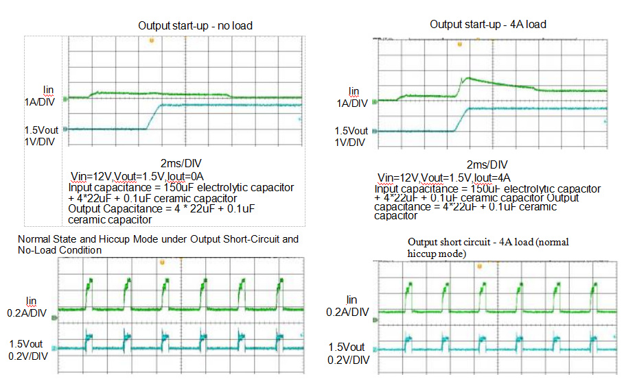
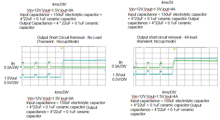
Output overcurrent protection
When the output current exceeds the current limit value, the FHT4644H enters the protection state. When the output current returns to the normal range, the converter enters the normal operating state.
Power Good
The PGOOD pin is an open drain pin that can be used to monitor each active output voltage. PG goes high when Vout falls below the set output voltage threshold. It can also be used to monitor protection functions such as UVLO and OTP, which can be monitored by pulling the resistor up to a specific supply voltage.
Over-temperature protection
When the case temperature of the FHT4644H rises above 135°C, it enters the over-temperature protection state.
Soldering and Storage Precautions
For lead-free BGA solder ball products, the peak temperature should not exceed 245℃; For leaded BGA solder ball products, the peak temperature should not exceed 225℃.
Recommended reflow soldering profile for reference recommended curves for reference:
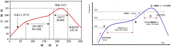
Lead Free Processes Leaded Processes
Caution:
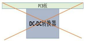
1.Due to the large size of the module, please do not place the module under the board for reflow soldering to avoid falling off.
2.For bulk products and those that have been taken out of their original packaging, they should be stored in a desiccator (with a relative humidity of less than 10% inside). For products still in their original packaging, they should also be stored in a desiccator whenever possible.
3.Before mounting on the board, it is necessary to strictly follow the baking conditions to dry the samples: bake at 125°C for more than 48 hours.
Regular size type
Product Model | Input | Output | Efficiency | Enable Voltage | Packaging | Grade | Temperature range (Case temperature) | Packaging | ||
Input Range | Nominal Input | Output range | Nominal Output | |||||||
FHT4644HIY | 4.0-14V | 12V | 0.6-5.5V | 5.0, 3.3, 2.5,1.5V | 92% | 1.2-14V | BGA (leaded) | industrial grade | -40-125°C | Tray |
FHT4644HIY#PBF | 4.0-14V | 12V | 0.6-5.5V | 5.0, 3.3, 2.5,1.5V | 92% | 1.2-14V | BGA (lead-free) | industrial grade | -40-125°C | Tray |
FHT4644HIV#PBF | 4.0-14V | 12V | 0.6-5.5V | 5.0, 3.3, 2.5,1.5V | 92% | 1.2-14V | LGA (lead-free) | industrial grade | -40-125°C | Tray |
FHT4644HMY | 4.0-14V | 12V | 0.6-5.5V | 5.0, 3.3, 2.5,1.5V | 92% | 1.2-14V | BGA (leaded) | general military grade | -55-125°C | Tray |
FHT4644HMY#PBF | 4.0-14V | 12V | 0.6-5.5V | 5.0, 3.3, 2.5,1.5V | 92% | 1.2-14V | BGA (lead-free) | general military grade | -55-125°C | Tray |
FHT4644HMV#PBF | 4.0-14V | 12V | 0.6-5.5V | 5.0, 3.3, 2.5,1.5V | 92% | 1.2-14V | LGA (lead-free) | general military grade | -55-125°C | Tray |
Ultra-thin size type
Product Model | Input | Output | Efficiency | Enable Voltage | Packaging | Grade | Temperature range (Case temperature) | Packaging | ||
Input Range | Nominal Input | Output range | Nominal Output | |||||||
FHT4644HLIY | 4.0-14V | 12V | 0.6-5.5V | 5.0, 3.3, 2.5,1.5V | 92% | 1.2-14V | BGA (leaded) | industrial grade | -40-125°C | Tray |
FHT4644HLIY#PBF | 4.0-14V | 12V | 0.6-5.5V | 5.0, 3.3, 2.5,1.5V | 92% | 1.2-14V | BGA (lead-free) | industrial grade | -40-125°C | Tray |
FHT4644HLIV#PBF | 4.0-14V | 12V | 0.6-5.5V | 5.0, 3.3, 2.5,1.5V | 92% | 1.2-14V | LGA (lead-free) | industrial grade | -40-125°C | Tray |
FHT4644HLMY | 4.0-14V | 12V | 0.6-5.5V | 5.0, 3.3, 2.5,1.5V | 92% | 1.2-14V | BGA (leaded) | general military grade | -55-125°C | Tray |
FHT4644HLMY#PBF | 4.0-14V | 12V | 0.6-5.5V | 5.0, 3.3, 2.5,1.5V | 92% | 1.2-14V | BGA (lead-free) | general military grade | -55-125°C | Tray |
FHT4644HLMV#PBF | 4.0-14V | 12V | 0.6-5.5V | 5.0, 3.3, 2.5,1.5V | 92% | 1.2-14V | LGA (lead-free) | general military grade | -55-125°C | Tray |
| Item | Description | Reel/Tray | Pcs/Roll | G.W | N.W | QTY/Carton | Package Size |
FHT4644 | Input 4.0V-15V, output 0.8V-5.5V DC/DC converters, each outputting 4A, capable of being paralleled for a total of 16A Ultra-thin SIP Packaged Power Module Efficiency up to 92% |
| 500pcs | 1.22kgs | 0.78kgs | 500pcs | 210*210*50mm |
Discover all the technical specifications by downloading the datasheet today.
| Part Number |
Output Current
(A) |
Input Voltage
(V) |
Output Voltage
(V) |
Dimensions(mm) |
Maximum
Efficienc |
Factory Pack
Quantity |
Footprint 3D | Datasheet | Sample |
| UDM2520I | 0.6A | 2.3V ~ 5.5V | 0.8V~3.3V | 2.5mm × 2mm x 1.1mm | 94% | 3,000pcs |  |
 |
|
| UDM22006 | 0.6A | 2.3V~5.5V | 1.2V~3.3V | 2.5mm x 2mm x 1.1mm | 95% | 3,000pcs | |
|
|
| UDM22010 | 1A | 2.3V ~ 5.5V | 1.2V ~ 3.3V | 2.5mm x 2mm x 1.1mm | 95% | 3,000pcs | |
|
|
| UDM82821adj | 1A | 2.5V~5.5V | 0.8V~4V | 2.5mm × 2mm x 1.1mm | 95% | 3,000pcs | |
|
|
| UDM82821 | 1.2A | 2.3V~5.5V | 1.2V~3.3V | 2.5mm × 2mm x 1.1mm | 95% | 3,000pcs | |
|
|
| UDM2826I | 1.5A | 2.7V ~ 5.5V | 1V ~ 3.3V | 2.8mm × 2.6mm x 1.1mm | 93% | 3,000pcs | |
|
|
| UDM3606 | 0.6A | 4.5V-18V | 0.6V-5.5V | 5mm×3.2mm×2.2mm | 95% | 3,000pcs | |
|
|
| UDM3506 | 0.6A | 4.7V-36V | 0.8V | 5mm×3.2mm×2.2mm | 88% | 3,000pcs | |
|
|
| UDM3610 | 1.2A | 4.5V~18V | 0.6V~5.5V | 5mm×3.2mm×2.2mm | 95% | 3,000pcs | |
|
|
| UDM92403 | 0.3A | 0.7V~5.5V | 1.8V~5.5V | 2.5mm×2mm x 1.1mm | 93% | 3,000pcs | |
|
|
| UDM81256 | 1A | 2.5V ~ 5.5V | 5V | 2.8mm×2.6mm×1.35mm(1.1mm) | 95% | 3,000pcs | |
|
|
| FHT4644 | 4A | 4.0V ~ 15V | 0.8V ~ 5.5V | 9mm x 15mm x 4.32mm | 92% | 500pcs | |
|
|
| FHT4644H | 4A | 4.0V ~14V | 0.6V ~ 5.5V | 9mmx15mmx4.32mm | 92% | 500pcs | |
|
|
| FHT4644C/D | 4A | 4.5V-14V | 0.6V-5.5V | 9mmx15mmx4.32mm | 92% | 500pcs | |
|
|
| FHT4644F | 4A | 4.5V ~ 16V | 0.6V ~ 5.5V | 9.0mmx15mmx4.32mm | 92% | 500pcs | |
|
|
| FHT4644L | 4A | 4.0V ~15V | 0.8V ~ 5.5V | 9mmx15mmx1.82mm | 92% | 500pcs | |
|
|
| FHT4630 | 18A+18A | 4.5V~15V | 0.6V ~ 1.8V | 16mm × 16mm × 5.01mm | 94% | 500pcs | |
|
|
| FHT3860 | 6A | 2.3V-5.5V | 0.5V-3.3V | 4mm x 6mm x 1.6mm | 94% | 500pcs | |
|
|
| FHM3695-25 | 20A | 4V-16V | 0.6V-5.5V | 10mm × 12mm ×4.32mm | 95% | 500pcs | |
|
|
| FHT4623 | 3A | 4.2V-20V | 0.6V-5.5V | 6.75mm x 6.75mm x 2.95mm | 95% | 500pcs | |
|
|
| MPPM8070 | 2A | 4.5V-18V | 0.6V-15V | 8mm×7mm × 4.32(2.5mm) | 93% | 500pcs | |
|
|
| FHT4618 | 6A | 4.5V-24V | 0.6V-5.5V | 15mm×9mm×4.32mm | 95% | 500pcs | |
|
|
| FHT23030 | 3A | 4.5V-17V | 0.9V-6V | 3mm×2.8mm×1.4mm | 94% | 500pcs | |
|
|
| FHT3550 | 5A | 3.5V-40V | 1.0V-12.0V | 12mm x 12mm x 4.32mm | 95% | 500pcs | |
|
|
| FHT8027C | 4A | 5V-60V | 2.5V-24V | 15mm×15mm×4.32mm | 95% | 500pcs | |
|

Data Centers and Server Farms

Medical Devices

Aerospace and Defense

Automotive Electronics

Industrial and Automation

Consumer Electronics
Telecommunications and Networking