

 Integrated Magnetic Power Module
Buck (Step-Down)-Low Voltage
Buck (Step-Down)-Medium Voltage
Boost (Step-Up)
DC-DC Power Modules
Integrated Magnetic Power Module
Buck (Step-Down)-Low Voltage
Buck (Step-Down)-Medium Voltage
Boost (Step-Up)
DC-DC Power Modules
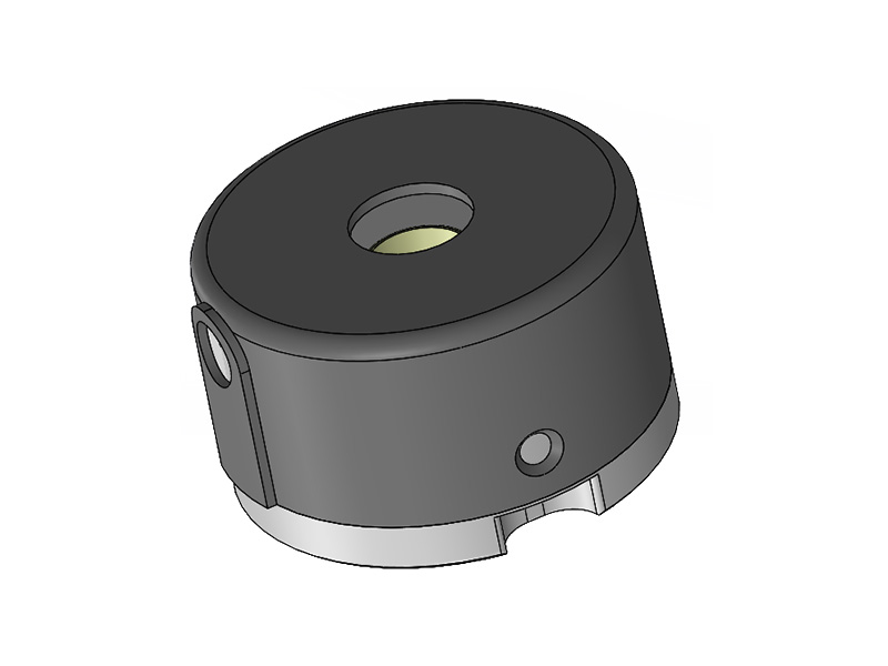
 Magnetically Integrated Power Module (SiP)
Buck (Step-Down)-Multiple Outputs
Buck (Step-Down)
Boost (Step-Up)
Magnetically Integrated Power Module (SiP)
Buck (Step-Down)-Multiple Outputs
Buck (Step-Down)
Boost (Step-Up)
 Customized DC-DC Converters
Tailored Power Modules: Precision Solutions for Your Unique Needs.
Contact Us Today to Discuss Your Project!

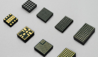
DC-DC Power Modules
Customized DC-DC Converters Explore DC-DC Converters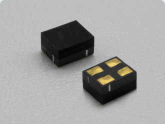
UDM22006 DC DC Integrated Magnetic Power Module ( Input 2.3V–5.5V, output 1.2V-3.3V )
Details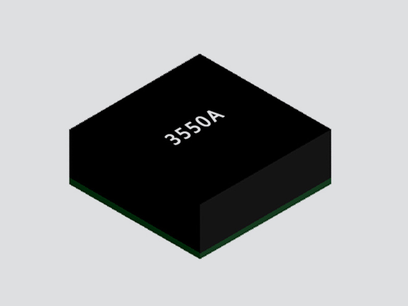
FHT3550 DC/DC Adjustable Buck Power Module ( 3.5V-40V Input, 1.0V-12.0V Output )
Details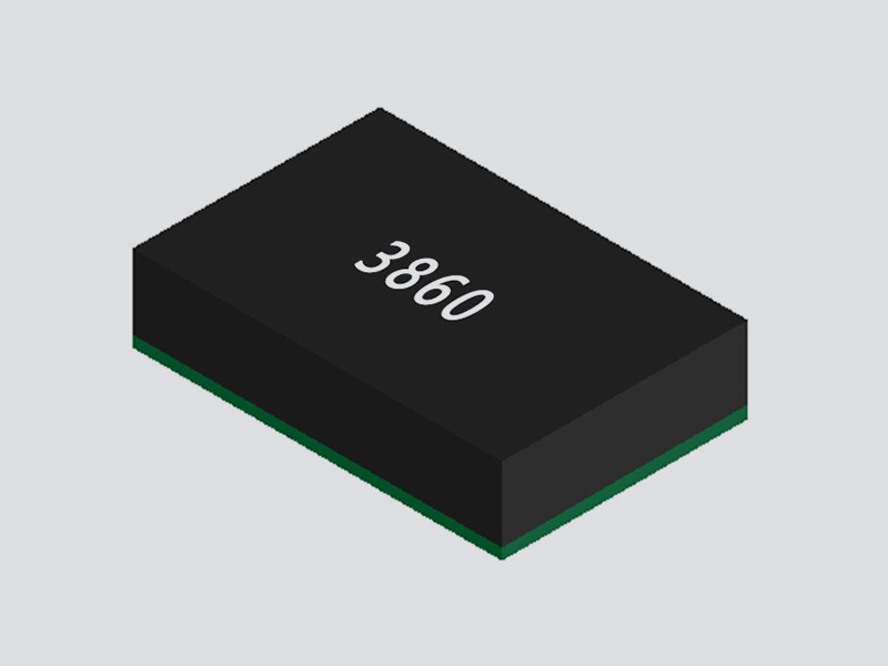
FHT3860 DC/DC Step-Down Buck Power Module ( 2.3V-5.5V Input, 0.5V-3.3V Output )
Details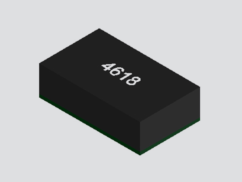
FHT4618 Integrated DC/DC Adjustable Buck Power Module ( 4.5V-24V Input, 0.6V-5.5V Output )
Details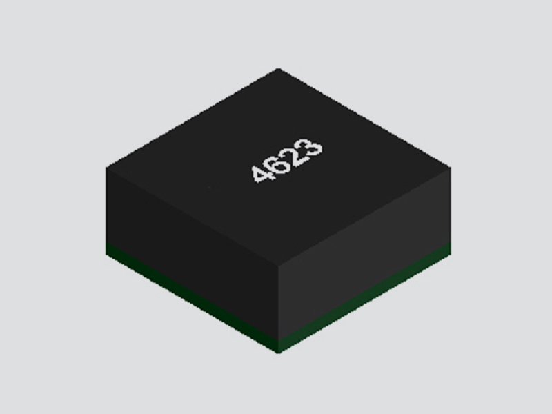
FHT4623 DC/DC Adjustable Buck Converter Power Module ( 4.2V-20V Input, 0.6V-5.5V Output )
Details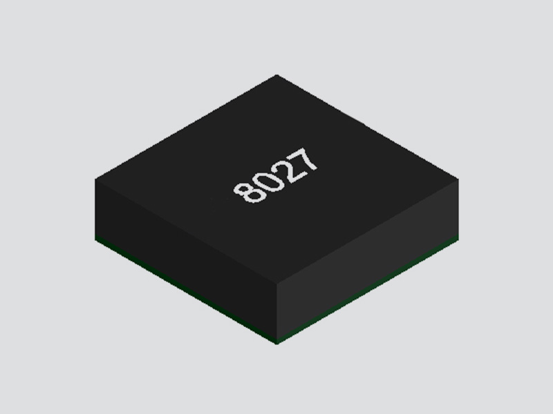
FHT8027C DC/DC Buck Converter Integrated Power Module ( 5V-60V Input, 2.5V-24V Output )
Details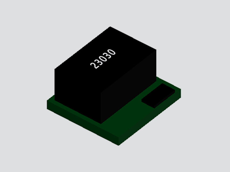
FHT23030 DC/DC Adjustable Buck Converter Module ( 4.5V–17V Input, 0.9V–6V Output )
Details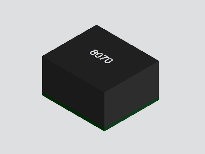
MPPM8070 DC/DC Adjustable Buck Converter Module ( Input 4.5V–18V, Output 0.6V-15V )
Details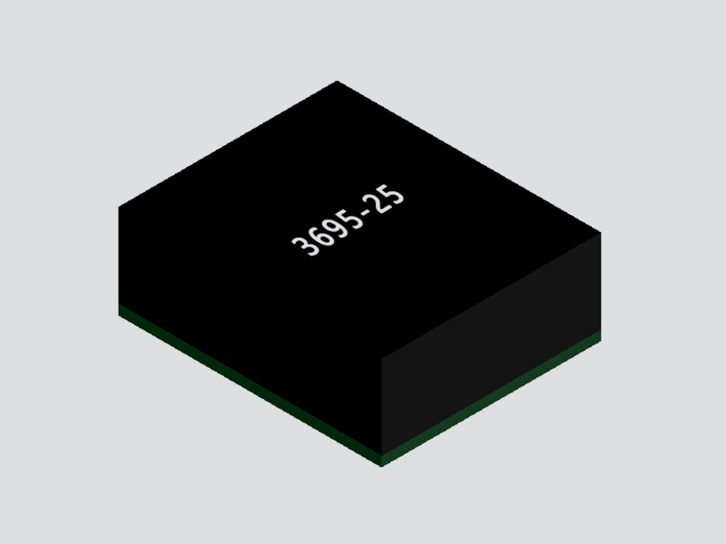
FHM3695 DC/DC Adjustable Buck Power Module ( 4V-16V Input, 0.6V-5.5V Output )
Details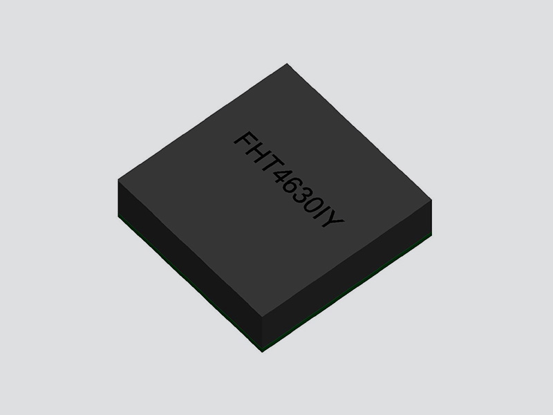
FHT4630 Dual-Channel DC/DC Adjustable Buck Converter Module ( 4.5V~15V Input, 0.6V ~ 1.8V Output )
Details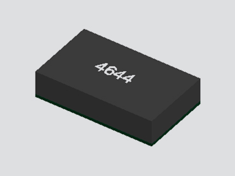
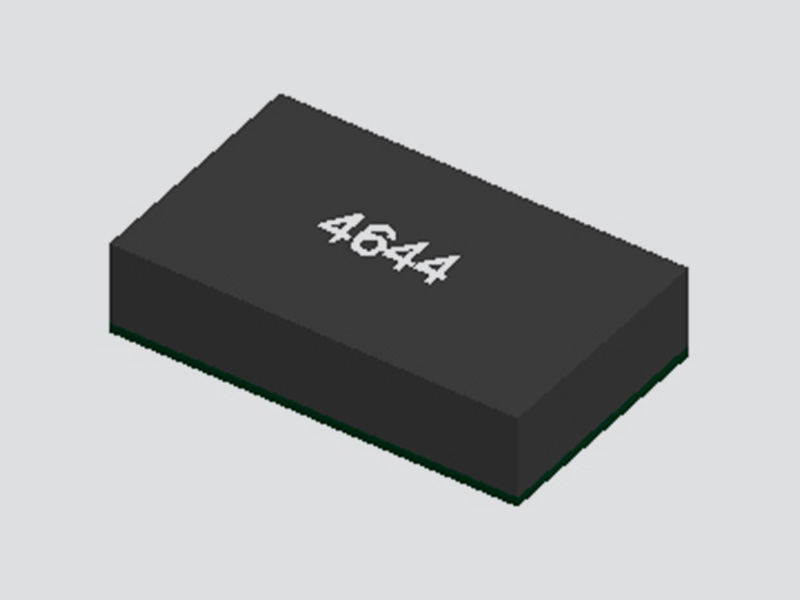
FHT4644C/D 4-Channel DC/DC Buck Power Module with Adjustable Outputs ( 4.5V-14V Input, 0.6V-5.5V Output )
Details
FHT4644F 4-Channel DC/DC Magnetically Integrated Buck Power Module (SiP) | 4.5V to 16V Input, 0.6V to 5.5V Output
Details
FHT4644H 4 Channel Integrated DC/DC Adjustable Buck Power Module ( 4.0V ~ 14V Input, 0.6V ~ 5.5V Output )
Details
FHT4644L 4-Channel Integrated Adjustable Buck DC/DC Power Module ( 4.0V ~ 15V Input, 0.8V ~ 5.5V Output )
Details
UDM2520I Integrated DC/DC Buck Step-Down Power Module ( 2.3V-5.5V Input, 0.8V-3.3V Output )
Details
UDM2826I Integrated DC-DC Buck Step-Down Power Module ( 2.7V-5.5V Input, 1.0V-3.3V Output )
Details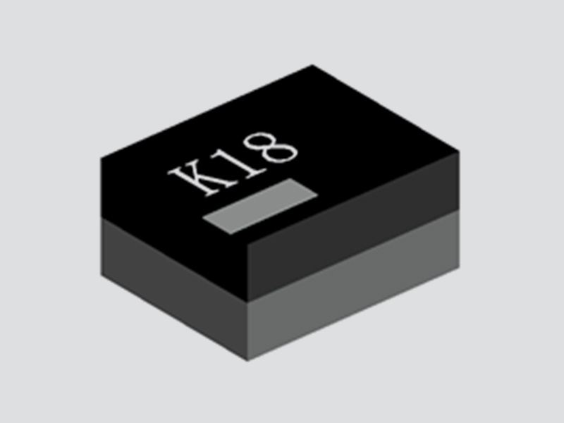
UDM22010 Integrated DC-DC Buck Step-Down Power Module ( 2.3V-5.5V Input, 1.2V-3.3V Output )
Details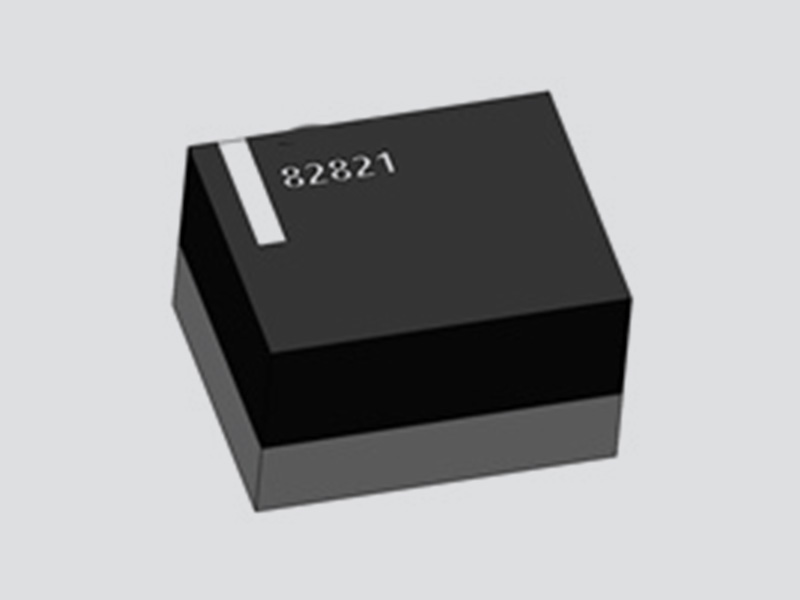
UDM82821 Integrated Magnetic DC-DC Buck Step-Down Power Module ( 2.3V-5.5V Input, 1.2V-3.3V Output )
Details
UDM82821adj Magnetically Integrated DC-DC Buck Power Module ( 2.5V-5.5V Input, 0.8V~4.0V Output )
Details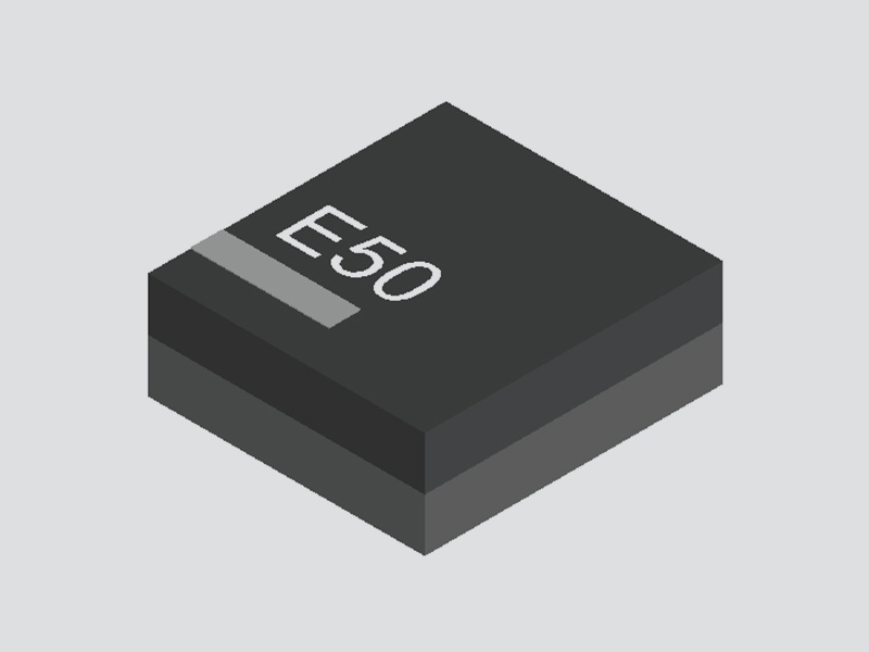
UDM81256 Integrated DC-DC Boost Power Module ( 2.5V-5.5V Input, Fixed 5V Output )
Details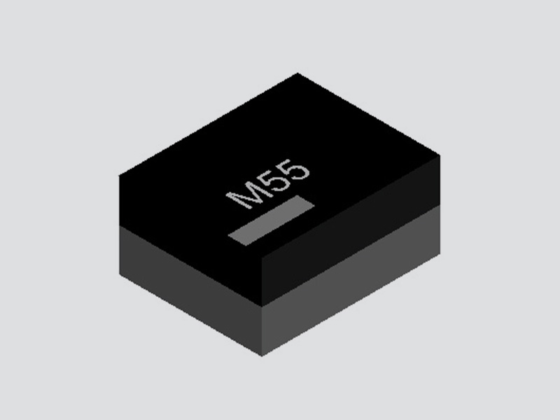
UDM92403 Integrated DC-DC Boost Step-Up Power Module ( 0.7V-5.5V Input, Adjustable 1.8V-5.5V Output )
Details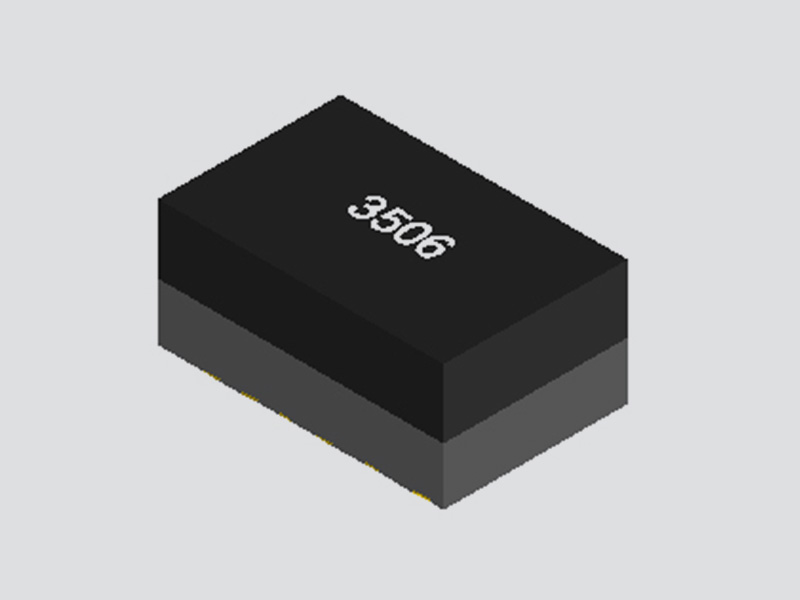
UDM3506 Integrated DC-DC Buck Step-Down Power Converter Module ( 4.7V-36V Input, 0.8V Output )
Details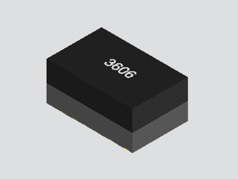
UDM3606 Integrated Medium Voltage DC-DC Buck Step-Down Power Module ( 4.5V-18V Input, 0.6V-5.5V Output )
Details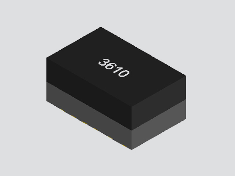
UDM3610 Integrated Medium Voltage DC-DC Buck Step-Down Power Supply Module ( 4.5V-18V Input, 0.6V-5.5V output )
DetailsUtilize SMT technology and SIP plastic-encapsulated packaging
General Specificatio: GJB 10164-2021
Detailed Specification: SC-Q/GZX52013-2022
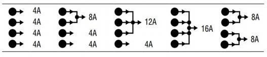
Output Current: Each channel provides a continuous full-load output current of 4A, with a peak of 5.5A
Parallel Connection: Four channels can be paralleled for a total output of 16A
Operating Temperature (Tc) :-55℃ ~ +125℃
Wide Input Voltage Range: 4.0V to 15V
Output Voltage Range:0.8V to 5.5V
Switching Frequency: Variable frequency, capable of automatic adjustment, typically 1MHz Operating Mode: Automatic adjustment mode Efficiency: 92%
No-load Power Consumption: The total for four channels is
0.01W (at 12Vin, 5V output)
Output Ripple Voltage: 15mVp-p (typical)
Voltage Regulation: ±1.0% (typical))
Load Regulation: ±0.5% (typical)
Soft-start: Internal 1ms soft-start (with an optional external 1ms soft-start)
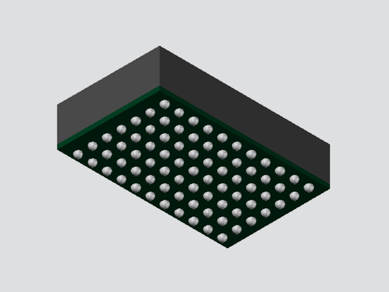
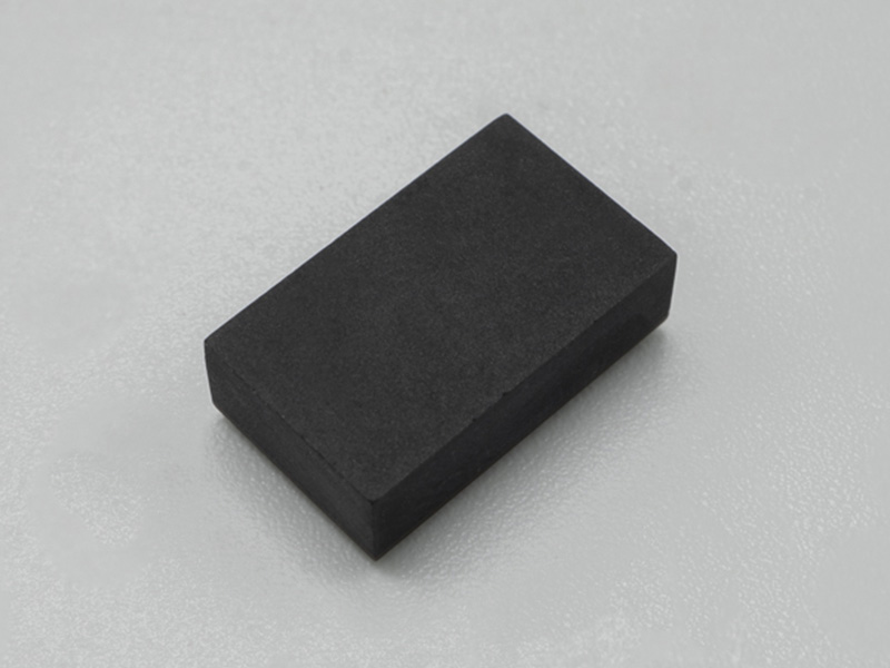
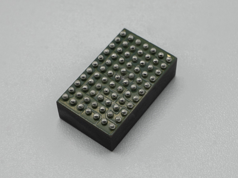
Protection Features: Protection against output overcurrent, overheating, output overvoltage, and input undervoltage Regular size: LGA package(9.0*15.0*4.32mm)
BGA package(9.0*15.0*5.01mm)
Ultra-thin size: LGApackage(9.0*15.0*1.82mm)
BGApackage(9.0*15.0*2.42mm)
Multi-rail Point-of-Load Regulation
Power Supply for CPUs and GPUs
Power Supply for ASIC Chips such as CPLDs, DSPs, and FPGAs
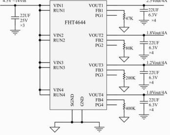
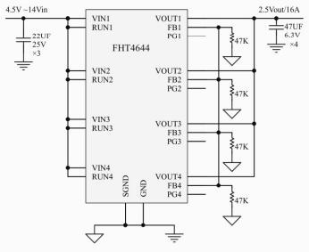
The FHT4644 is a non-isolated buck DC/DC power module with a wide input voltage range of 4 to 15V and an adjustable output voltage of 0.8 to 5.5V. It features four output channels, each capable of delivering up to 4A, and offers users the choice of LGA and BGA packaging options. The FHT4644 is an SMT surface-mount module that is welded onto the PCB board using reflow soldering.
It boasts high power density and a compact size, with an ultra-thin thickness of only 1.82mm and a power density reaching 300W/cm³. The power module circuit integrates the power supply chip, inductor, and related components, allowing for the rapid design of a multi-channel power supply system by simply configuring a voltage-adjusting resistor and a few input/output ceramic capacitors for each output channel. This simplified system design maximizes PCB layout space savings. As a point-of-load power supply, the FHT4644 can be directly mounted next to the FPGA, providing high-precision voltages such as 5.0V, 3.3V, 2.5V, and 1.2V for digital circuits, FPGA control circuits, motherboards, CPUs, communication systems, storage, and other components in the system. Each channel can continuously provide a current of 4A, and the four output channels can be combined and used in parallel, as well as paralleled with other FHT4644 power modules.
It is ideally suited for applications requiring low output voltages and multiple channels. The operating mode and frequency of the FHT4644 can be automatically adjusted based on real-time input and output voltages and loads, which not only simplifies the peripheral circuitry but also minimizes no-load power consumption, ensuring that the power module always operates in the optimal state. All components of the FHT4644 are domestically produced, and an autonomous and controllable report can be provided. Additionally, this power module is characterized by high reliability,high efficiency, and long life. Especially when outputting low voltages, its efficiency is significantly higher than similar products, providing a more reliable and stable power supply for the system.
Configurable output array
Non-parallel Application
Parallel Application
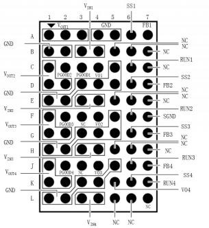
| Pin | Description |
VOUT1(A1,A2,A3),VOUT2(C1,D1,D2) VOUT3(F1,G1,G2), VOUT4(J1,K1,K2), | Power Module Quad Output Pins |
| VIN1(B3,B4),VIN2(E3,E4),VIN3(H3,H4),VIN4(L3,L4) | Power Module Quad Input Pins |
GND(A4,A5,B1,B2,C5,D3,D4,D5,E1,E2,F5,G3,G4,G5,H1,H2, J5,K3,K4,L1,L2) | Ground pin |
| FB1(A7),FB2(D7),FB3(G7),FB4(J7) | The four output voltage adjustment pins can be connected to GND with 0.5% accuracy voltage adjustment resistors. |
| RUN1(C6),RUN2(F6),RUN3(J6),RUN4(K7) | The four enable pins can be directly connected to the input voltage,or connected to an extemal power supply to control the power module.The minimum enable voltage is 1.1V,and when the enable voltage is lower than 0.95V, the power supply will be turned off.It is recommended that the enable voltage is greater than 1.2V,this pin can not be suspended. |
| PGOOD1(C3),PGOOD2(C2),PGOOD3(F2),PGOOD4(J2) | The fault indicator pin,PG=High indicates that VOUT is within the voltage range, while PG=Low indicates that VOUT is below the specified value.The PGOOD pin can be connected to the VO pin through a 100K resistor (note:it is necessary to evaluate whether the actual voltage at the VO pin meets the voltage requirements of the subsequent FPGA or other chip VO ports).Altematively,an extemal voltage can be supplied to PGOOD.When PGOOD is set to Low, t indicates an abnormality in the power module (including undervoltage (UV),overvoltage (OV),overcurrent(OC), overtemperature(OT),etc.).If the fault indication function is not required,this resistor can be omitted,and PGOOD can be left floating |
| VO1(C4),VO2(F4),VO3(J4),VO4(K5) | VO can serve as the power supply pin for PG.The four sets of VO have been respectively connected to the four output terminals within the power module,i.e., VO1=VOUT1,VO2=VOUT2,VO3=VOUT3,and VO4=VOUT4. |
| MODE1(B6),MODE2(E6),MODE3(H6),MODE4(L6) | Unused pins,without electrical function,can be connected to any pin. (The FHT4644 can automatically adjust its operating frequency and mode, with a typical operating frequency of 1MHz.) |
| SGND(F7) | Signal ground.It is recommended to separate the wiring of GND(power ground) and SGND,and ultimately connect them using a 0-ohm resistor. |
| SS1(A6),SS2(D6),SS3(G6),SS4(K6) | External soft-start pin.An external 3.3nF ceramic capacitor can be connected to the signal ground.If the external soft-start function is not required,this capacitor can be omitted,and the SS pin can be left floating. |
| NC(E7,H7,L7,C7,L5,H5,E5,B5,J3,F3) | Unused pin without electrical function,it can be connected to any pin. |
Limit Value | Condition | Minimum value | Nominal value | Maximum value | Unit |
VIN(each way) | -0.3 | 17 | V | ||
FB、VOUT(each way) | -0.3 | 7 | V | ||
PGOOD(each way) | -0.3 | 12 | V | ||
PGOOD(each way) | 10 | mA | |||
VO,SS/TR(each way) | -0.3 | 7 | V | ||
RUN(each way) | -0.3 | 17 | V | ||
Storage temperature | -55 | 150 | ℃ | ||
Reflow temperature | 245 | ℃ | |||
Input Characteristics | Condition | Minimum value | Nominal value | Maximum value | Unit |
Input Voltage Range | 4.0 | 12 | 14 | V | |
Power-on voltage threshold | 3.95 | V | |||
Shutdown Voltage Threshold | 3.5 | 3.6 | 3.9 | V | |
Input current at full load | VIN =12V,VOUT =1.5V,IOUT =4A | 0.6 | A | ||
Input current at low voltage full load | VIN =5V,VOUT =1.5V,IOUT =4A | 1.5 | A | ||
Input current at no load | VIN =12V,VOUT =1.5V,IOUT =0A | 650 | μA | ||
Static Input Current | ON/OFF=OFF | 15 | μA | ||
General Requirements | Condition | Minimum Value | Nominal Value | Maximum Value | Unit |
Switching Frequency | Automatic Adjustment | 1000 | KHz | ||
Efficiency | Vin=5V , Vout=3.3V | 92 | % | ||
Soft Start Time | SS pin with 3.3nF ceramic capacitor | 2 | ms | ||
Enable | Condition | Minimum value | Nominal value | Maximum value | Unit |
RUN enable voltage | 1.2 | - | 14 | V | |
Output Characteristics | Condition | Minimum value | Nominal value | Maximum value | Unit |
Output Voltage Range | Adjusted by FB pin resistor | 0.8 | 5.5 | V | |
Output Voltage | CIN = 22µF, COUT = 22uF×4,VIN = 4V to 14V, IOUT = 0A to 4A |
1.47 |
1.5 |
1.53 | V |
Linear Regulation | VOUT = 1.5V , 4V < VIN < 14V , ILOAD = 4A | ±0.5 | ±1 | % | |
Load Regulation | VIN =12V , VOUT =1.5V,1A < ILOAD ≤ 4A | ±1 | ±2 | % | |
Ripple and Noise | VIN =12V , VOUT =1.5V , IOUT =4A, Cout =22uF×4 , 20MHz bandwidth |
10 |
50 |
mV | |
Dynamic Load Response | 75-100% full load , di/dt = 1A/μS Cout =22uF×4 | 50 ,40 | mV ,µs |
Output Characteristics | Condition | Minimum value | Nominal value | Maximum value | Unit |
Output Overcurrent Protection | Iout% | 115 | 120 | 125 | % |
Output Overvoltage Protection | Vout% | 115 | 115 | 130 | % |
Over-Temperature Protection | Case temperature(Tc) | - | - | 135 | ℃ |
Structural Characteristics | Conditions | Minimum Value | Nominal value | Maximum value | Unit |
Packaging | LGA、BGA | - | - | - | - |
Standard Size | LGA: 9*15*4.32; BGA: 9*15*5.01 | - | - | - | mm |
Ultra-thin Size | LGA: 9*15*1.82; BGA: 9*15*2.42 | - | - | - | mm |
Weight | 1.6 | g | |||
Environmental Adaptability | Condition | Minimum value | Nominal value | Maximum value | Unit |
Operating temperature (Case temperature) | -55 | 125 | ℃ | ||
High temperature storage (ambient temperature) | +125℃, 48h | 125 | ℃ | ||
High temperature operation (ambient temperature) | +85℃, 24h; Input: 8 hours each for low voltage, standard voltage, load derating, and high voltage | 85 | ℃ | ||
Low temperature storage (ambient temperature) | -55℃, 24h | -55 | ℃ | ||
Low temperature operation (ambient temperature) | -55℃, 24h; nput low pressure, standard pressure, high pressure each 8h | -55 | ℃ | ||
Damp heat | High temperatu re and high humidity stage: 60℃, 95%; Low temperature and high humidity stage: 30℃, 95%; 10 cycles, each cycle is 24h. | 30 | 60 | ℃ | |
Temperature shock | High temperature 125 ℃, low temperature -55 ℃, high and low temperature of an hour for a cycle, a total of 32 cycles of the test | -55 | 125 | ℃ |
NOTE : Stresses above the values listed in the "Limit Values" section may cause permanent damage to the device. Prolonged exposure to any of the absolute maximum ratings may affect the reliability and life of the device.


FHT4644 is a four-channel independent output non-isolated DC/DC switching regulator. It has four independent regulator channels, each capable of providing up to 4A of continuous output current, requiring only a small amount of external
input and output capacitance. Within the input voltage range of 4.0V to 15V, each regulated channel can provide an accurately regulated output voltage through an external resistor, with a voltage range of 0.8V to 5.5V.
RUN Start
Pulling the RUN pin of each regulator channel to ground forces the regulator into shutdown mode, turning off the power MOSFET and most of the internal control circuits. Keeping the RUN pin above 0.7V only turns on the internal reference while still keeping the power MOSFET off. Further increasing the RUN pin voltage above 1.2V will turn on the entire regulator channel.
The output voltage setting is internal to the FHT4644, with the FB pin connected to the VOUT terminal of each channel through a 100kΩ precision resistor. The output voltage of this module can be adjusted by the resistor RFB between FB and GND, with the calculation as follows::

Note 1: It is recommended to reserve two resistor positions with a precision of 0.5% for fine-tuning the output voltage.
Below is List 1, which shows the relationship between the RFB resistor and various output voltages:
Vout (V) | 0.8 | 1.0 | 1.2 | 1.5 | 1.8 | 2.5 | 3.3 | 5.0 |
RFB (kΩ) | open | 400 | 200 | 114.3 | 80 | 47.06 | 32 | 19.05 |
Note 2: When used in parallel, such as N parallel circuits, the RFB resistor value at this time is the single-channel RFB resistor value divided by N. For example, when four circuits are paralleled for a 3.3V output, the RFB resistor value would be 32kΩ divided by 4, which equals 8kΩ.
Soft Start
The FHT4644 module incorporates a built-in soft-start feature with a duration of 1 millisecond (mS). Additionally, an external soft-start pin is available for selection, allowing for increased delay time by connecting a ceramic capacitor of approximately 3.3 nanofarads (nF). The following formula can be used to calculate the soft-start capacitor value:Css=4XT SS
Css represents the capacitance value of the soft-start capacitor, measured in nanofarads (nF). Tss stands for the soft-start time, measured in milliseconds (mS). For example, when an additional soft-start time of 1 millisecond is desired, the required soft-start capacitor would be 4 nanofarads.
Input Under-Voltage Protection
The FHT4644 features input under-voltage protection. When the VIN (input voltage) drops below 3.7V, the under-voltage lockout (UVLO) function is activated.
Note: If the input cable is relatively long, there may be a voltage drop along the cable due to resistance. To ensure normal output, it is necessary to guarantee that the voltage at the module's input pin is greater than 4.0V.
Output Over-Current Protection
The FHT4644 also incorporates output over-current protection. When the output current exceeds the preset current limit, the converter enters a protection state to prevent damage to the load or the converter itself. Once the output current returns to within the normal range, the converter automatically resumes normal operation.
Power Good
The PGOOD pin is an open-drain pin that can be used to monitor each valid output voltage. When the Vout falls below the threshold voltage set for the output voltage, the PGOOD pin goes high. It can also be used to monitor protective functions such as UVLO (Under-Voltage Lockout) and OTP (Over-Temperature Protection). By connecting a resistor to pull the PGOOD pin up to a specific supply voltage, monitoring can be achieved.
Below is a schematic diagram of the PGOOD circuit, and List 2 provides the logic table for the PGOOD pin:

Monitoring Items | Conditions | PG States |
UVLO | 0.7V<VIN<VUVLO | Low Level |
On(RUN =High Level) | VFB≥VTH_PG | High Level |
VFB≤VTH_PG | Low Level | |
Off (RUN=High Level | Low Level | |
Temperature Protection Shutdown | TJ>TSD | Low Level |
Power Removal | VIN<0.7V | High Level |
VFB stands for the voltage feedback pin voltage, VTH_PG represents the PGOOD threshold voltage, TJ denotes the junction temperature, and TSD signifies the temperature at which the power supply protection shutdown occurs.
Over-Temperature Protection
When the case temperature of the FHT4644 rises above 135°C, it enters an over-temperature protection state.
Package Description

1、Recommended Operating Conditions for This Module:
★Input Voltage Range:VIN = 4.0V~ 15V(It is recommended that the minimum input voltage be greater than 4.2V)
★ Output Voltage Range:VOUT = 1.0V~5.0V
★ Output Current Range: (Recommendation for 80% Derating Usage))
Iout= 0~4A Operating independently in a single channel
Iout=N ×( 0~4A) N represents the number of parallel channels
★ Operating Case Temperature TC: -55℃ ~ 125℃
2、Testing and Application Instructions
It is not recommended to use a linear power supply for functional testing of this power module (as linear power supplies tend to generate transient voltage fluctuations when adjusting the output, posing a risk of exceeding the maximum rated voltage). Instead, it is recommended to use a switching power supply or a DC/DC module power supply.
★ This power module features a high power density circuit, and it is recommended to use a PCB board with 4 layers or more for layout. Considering long-term stable operation under high temperature conditions, it is advisable to implement appropriate load derating (80% of rated load) or thermal management measures (options include: system-level air cooling, attaching a heatsink above the power module, increasing the copper-clad area on the PCB board beneath the power module, etc.).
★ For the PCB board application of this power module, it is recommended to use wider copper foil for the layout of VIN, VOUT, and GND to reduce conduction losses and thermal stress caused by high currents. It is advisable to place the input and output filtering capacitors close to the power module. To avoid interference, it is recommended to layout the input capacitors and output capacitors with a distance greater than 1 cm between them.
★ If you were previously using an LTM4644 peripheral circuit design, you will need to recalculate RFB according to the following formula.,Only the resistance value needs to be changed, and there is no need to modify the PCB layout.

★ This power module is a hermetically sealed product. Before soldering, check the changes on the humidity indicator card to determine if pre-baking treatment is necessary.
★ Attention should be paid to electrostatic protection during product transportation.
Operating Conditions、Testing and Special Application Notes
3、Thermal Derating Curve Reference Diagram (Load Current vs. Ambient Temperature, Tested in Temperature Chamber, Without Additional Cooling Devices, Evaluating Loading Conditions of Power Supply Module at Different Ambient Temperatures)

4、Thermal Derating Curve Reference Diagram (Load Current vs. Case Temperature, Tested at Room Temperature, Without Additional Cooling Devices, Evaluating the Rise in Case Temperature of the Power Supply Module Under Different Load Conditions)

Precautions for Reflow Soldering
1. Products that are well-packaged must undergo baking at 125°C for 24 hours before use. If the packaging bag is found to be torn or if the desiccant or indicator label has changed color, the products must undergo baking at 125°C for 48 hours before use. For more information, please refer to the IPC/JEDEC J-STD-033 standard.
2. For reflow soldering of lead-free BGA solder ball products, the peak temperature should not exceed 245°C; for lead-containing BGA solder ball products, the peak temperature should not exceed 225°C.
3. It is recommended to use a stencil thickness of 125um-160um, with stencil openings slightly smaller than the solder pads. Taking a Φ0.635mm solder pad as an example, the recommended stencil opening size is Φ0.620mm.
4. The solder paste can be either lead-free SAC or SnPb (with lead). Powder types 3 or 4 are recommended. Different brands of solder paste may have different welding recommendations, so please pay attention to the references. The porosity rate is recommended to not exceed 25%.
Recommended Reflow Soldering Parameters Table
Lead-free solder paste | SnPb (lead-containing) solder paste | ||
Preheat | Minimum Preheat Temperature | 150℃ | 100℃ |
Maximum Preheat Temperature | 200℃ | 150℃ | |
Preheat Duration | (60-120)seconds | (60-120)seconds | |
Reflow Soldering | Melting Point | 217℃ | 183℃ |
Duration Above Melting Point | (30-90)seconds | (30-90)seconds | |
Peak Temperature of the Welding Curve | 245℃ | 225℃ | |
Maximum Duration within ±5℃ of Peak Temperature | 30 seconds | ||
Maximum Average Heating Rate | 2.5℃/second | ||
Maximum Cooling Rate | 2.5℃/second | ||
Maximum Time to Reach Peak Temperature from 25℃ | 8 minutes |
Recommended Reflow Soldering Profile (for reference)

Appendix I: Key Differences and Explanation between FHT4644 and LTM4644
Functional Differences
LTM4644 | FHT4644 | |
Input Voltage | 4-14V | 4-14V |
Output Voltage | 0.6-5.5V | 0.8-5.5V |
Operating Frequency | Nominal value of 1M, externally adjustable | Nominal value of 1M, automatically adjustable |
Operating Mode | CCM/DCM adjustable | CCM/DCM automatically adjustable |
Total Output Voltage Regulation | ±1.5%(Typical Value) | ±1.5%(Typical Value) |
Output Voltage Setting | FB=0.6V, R1=60.4K | FB=0.8V, R1=100K |
Output Voltage Tracking | Yes | Yes |
Output Clock Signal | Yes | Internal power supply chip |
Internal Temperature Sensing | Yes | Internal power supply chip |
Stability Compensation | Yes | Internal power supply chip |
Dimensions | 9mm×15mm×5.01mm | 9mm×15mm×5.01mm |
Note: Due to differences in the calculation formula for the external voltage regulation resistor, the resistance
values of the voltage regulation resistors for FHT4644 and LTM4644 are not the same.
FHT4644 voltage regulation resistance calculation formula and voltage regulation resistance value list:

LTM4644 voltage regulation resistance calculation formula and voltage regulation resistance value list:

2. Pin Configuration Comparison
Pin | LTM4644 | FHT4644 |
Same Pin Configuration | ||
Input | VIN1(B3,B4), VIN2(E3,E4), VIN3( H3,H4), VIN4(L3,L4) | VIN1(B3,B4), VIN2(E3,E4), VIN3( H3,H4), VIN4(L3,L4) |
Output | VOUT1(A1,A2,A3), VOUT2(C1,D1,D2), VOUT3(F1,G1,G2), VOUT4(J1,K1,K2) | VOUT1(A1,A2,A3), VOUT2(C1,D1,D2), VOUT3(F1,G1,G2), VOUT4(J1,K1,K2) |
Ground Pin | GND(A4,A5, B1,B2, C5, D3,D4,D5, E1,E2, F5, G3,G4,G5, H1,H2, J5,K3, K4,L1,L2) | GND(A4,A5, B1,B2, C5, D3,D4,D5, E1,E2, F5, G3,G4,G5, H1,H2, J5,K3, K4,L1,L2) |
Feedback Pin | FB1(A7), FB1(D7),FB3(G7), FB4(J7) | FB1(A7), FB2(D7),FB3(G7), FB4(J7) |
Enable Pin, | RUN1(C6), RUN2(F6) RUN3(J6), RUN4(K7) | RUN1(C6), RUN(F6), RUN3(J6), RUN4(K7) |
PG Signal | PGOOD1( C3),PGOOD2( C2), PGOOD3(F2),PGOOD4(J2) | PGOOD1( C3),PGOOD2( C2), PGOOD3(F2),PGOOD4(J2) |
Signal Ground | SGND(F7) | SGND(F7) |
Soft Start and Output Voltage Tracking Pin | SS1/TRACK1(A6),SS2/TRACK2(D6), SS3/TRACK3 (G6),SS4/TRACK4 (K6) | SS1/TRACK1(A6),SS2/TRACK2(D6), SS3/TRACK3 (G6),SS4/TRACK4 (K6) |
Pin | LTM4644 | FHT4644 |
Different Pin Configuration | ||
Mode Select Pin | MODE1(B6), MODE2(E6), MODE3(H6), MODE4(L6) | B6, E6, H6, L6 are left floating and are not required. The mode can be automatically adjusted。 |
INTvcc (Internal Voltage Source) | INTvcc1(C4), INTvcc1( F4), INTvcc1(J4), INTvcc1(K5) | VO1(C4),VO2(F4) ,VO3(J4), VO4(K5) ,There is no INTvcc, and the PG power supply can be provided by the VO pin,VO=Vout。 |
Svin (Internal Power Supply) | SVIN1, SVIN2, SVIN, SVIN4 (B5, E5, H5, L5) | B5, E5, H5, L5 are left floating, and the internal power supply chip does not require SVIN |
Stability Compensation Pin | COMP1, COMP2, COMP3, COMP4 (B7, E7, H7, L7) | B7, E7, H7, L7 are left floating and are not required as they are already integrated into the power supply chip |
Output Clock Signal | CLKOUT (J3) | Left floating, not required, automatically adjustable. |
ync Signal | CLKIN(C7):External synchronization input module detector for phase. | Left floating, not required, automatically adjustable. |
Junction Temperature Sense Pin | TEMP (F3) | Left floating, the power supply chip has built-in over-temperature protection. |
Through the above comparison, due to the automatic frequency conversion technology adopted by FHT4644, the operating mode does not require additional circuit control, and the peripheral circuitry is simpler than that of LTM4644. This allows for more component layout savings. By simply changing the voltage regulation resistor RFB, FHT4644 can be used as a drop-in replacement for LTM4644 without the need to modify the existing PCB layout.
1. Product Naming Convention
FHT 4644 L M Y #PBF
① ② ③ ④ ⑤ ⑥
① Manufacturer Code
② Product Series Number
③ The presence of "L" signifies an ultra-thin size model, while its absence indicates a regular size model
④ Usage Grade: "M" stands for Military Grade (general military use), "I" for Industrial Grade, and "E" for Consumer Grade
⑤ Lead Configuration: "Y" or "V". "V" represents Land Grid Array (LGA) packaging, while "Y" represents Ball Grid Array
(BGA) packaging
⑥BGA Solder Ball Characteristics: "#PBF" indicates lead-free, while the absence of this notation signifies lead-based
Product Model | Input | Output | Efficiency | Enable Voltage | Packaging | Grade | Temperature Range (Case Temperature) | Packaging | ||
Input Range | Nominal Input | Output range | Nominal Output | |||||||
FHT4644MY | 4.0-15V | 12V | 0.8-5.5V | 5.0 ,3.3, 2.5,1.5V | 92% | 1.2-15V | BGA | general military grade | -55-125℃ | Tray |
FHT4644MY#PBF | 4.0-15V | 12V | 0.8-5.5V | 5.0 ,3.3, 2.5,1.5V | 92% | 1.2-15V | BGA | general military grade | -55-125℃ | Tray |
FHT4644MV#PBF | 4.0-15V | 12V | 0.8-5.5V | 5.0 ,3.3, 2.5,1.5V | 92% | 1.2-15V | LGA | general military grade | -55-125℃ | Tray |
FHT4644IY | 4.0-15V | 12V | 0.8-5.5V | 5.0 ,3.3, 2.5,1.5V | 92% | 1.2-15V | BGA | industrial grade | -40-125℃ | Tray |
FHT4644IY#PBF | 4.0-15V | 12V | 0.8-5.5V | 5.0 ,3.3, 2.5,1.5V | 92% | 1.2-15V | BGA | industrial grade | -40-125℃ | Tray |
FHT4644IV#PBF | 4.0-15V | 12V | 0.8-5.5V | 5.0 ,3.3, 2.5,1.5V | 92% | 1.2-15V | LGA | industrial grade | -40-125℃ | Tray |
FHT4644EY#PBF | 4.0-15V | 12V | 0.8-5.5V | 5.0 ,3.3, 2.5,1.5V | 92% | 1.2-15V | BGA | Consumer Grade | -40-125℃ | Tray |
FHT4644LMY | 4.0-15V | 12V | 0.8-5.5V | 5.0 ,3.3, 2.5,1.5V | 92% | 1.2-15V | BGA (leaded) | general military grade | -55-125℃ | Tray |
FHT4644LMY#PBF | 4.0-15V | 12V | 0.8-5.5V | 5.0 ,3.3, 2.5,1.5V | 92% | 1.2-15V | BGA (lead-free) | general military grade | -55-125℃ | Tray |
FHT4644LMV#PBF | 4.0-15V | 12V | 0.8-5.5V | 5.0 ,3.3, 2.5,1.5V | 92% | 1.2-15V | LGA (lead-free) | general military grade | -55-125℃ | Tray |
FHT4644LIY | 4.0-15V | 12V | 0.8-5.5V | 5.0 ,3.3, 2.5,1.5V | 92% | 1.2-15V | BGA (leaded) | industrial grade | -40-125℃ | Tray |
FHT4644LIY#PBF | 4.0-15V | 12V | 0.8-5.5V | 5.0 ,3.3, 2.5,1.5V | 92% | 1.2-15V | BGA (lead-free) | industrial grade | -40-125℃ | Tray |
FHT4644LIV#PBF | 4.0-15V | 12V | 0.8-5.5V | 5.0 ,3.3, 2.5,1.5V | 92% | 1.2-15V | LGA (lead-free) | industrial grade | -40-125℃ | Tray |
FHT4644LEY#PBF | 4.0-15V | 12V | 0.8-5.5V | 5.0 ,3.3, 2.5,1.5V | 92% | 1.2-15V | BGA (lead-free) | Consumer Grade | -40-125℃ | Tray |
| Item | Description | Reel/Tray | Pcs/Roll | G.W | N.W | QTY/Carton | Package Size |
FHT4644 | Input 4.0V-15V, output 0.8V-5.5V DC/DC converters, each outputting 4A, capable of being paralleled for a total of 16A Ultra-thin SIP Packaged Power Module Efficiency up to 92% |
| 500pcs | 1.22kgs | 0.78kgs | 500pcs | 210*210*50mm |
Discover all the technical specifications by downloading the datasheet today.
| Part Number |
Output Current
(A) |
Input Voltage
(V) |
Output Voltage
(V) |
Dimensions(mm) |
Maximum
Efficienc |
Factory Pack
Quantity |
Footprint 3D | Datasheet | Sample |
| UDM2520I | 0.6A | 2.3V ~ 5.5V | 0.8V~3.3V | 2.5mm × 2mm x 1.1mm | 94% | 3,000pcs |  |
 |
|
| UDM22006 | 0.6A | 2.3V~5.5V | 1.2V~3.3V | 2.5mm x 2mm x 1.1mm | 95% | 3,000pcs | |
|
|
| UDM22010 | 1A | 2.3V ~ 5.5V | 1.2V ~ 3.3V | 2.5mm x 2mm x 1.1mm | 95% | 3,000pcs | |
|
|
| UDM82821adj | 1A | 2.5V~5.5V | 0.8V~4V | 2.5mm × 2mm x 1.1mm | 95% | 3,000pcs | |
|
|
| UDM82821 | 1.2A | 2.3V~5.5V | 1.2V~3.3V | 2.5mm × 2mm x 1.1mm | 95% | 3,000pcs | |
|
|
| UDM2826I | 1.5A | 2.7V ~ 5.5V | 1V ~ 3.3V | 2.8mm × 2.6mm x 1.1mm | 93% | 3,000pcs | |
|
|
| UDM3606 | 0.6A | 4.5V-18V | 0.6V-5.5V | 5mm×3.2mm×2.2mm | 95% | 3,000pcs | |
|
|
| UDM3506 | 0.6A | 4.7V-36V | 0.8V | 5mm×3.2mm×2.2mm | 88% | 3,000pcs | |
|
|
| UDM3610 | 1.2A | 4.5V~18V | 0.6V~5.5V | 5mm×3.2mm×2.2mm | 95% | 3,000pcs | |
|
|
| UDM92403 | 0.3A | 0.7V~5.5V | 1.8V~5.5V | 2.5mm×2mm x 1.1mm | 93% | 3,000pcs | |
|
|
| UDM81256 | 1A | 2.5V ~ 5.5V | 5V | 2.8mm×2.6mm×1.35mm(1.1mm) | 95% | 3,000pcs | |
|
|
| FHT4644 | 4A | 4.0V ~ 15V | 0.8V ~ 5.5V | 9mm x 15mm x 4.32mm | 92% | 500pcs | |
|
|
| FHT4644H | 4A | 4.0V ~14V | 0.6V ~ 5.5V | 9mmx15mmx4.32mm | 92% | 500pcs | |
|
|
| FHT4644C/D | 4A | 4.5V-14V | 0.6V-5.5V | 9mmx15mmx4.32mm | 92% | 500pcs | |
|
|
| FHT4644F | 4A | 4.5V ~ 16V | 0.6V ~ 5.5V | 9.0mmx15mmx4.32mm | 92% | 500pcs | |
|
|
| FHT4644L | 4A | 4.0V ~15V | 0.8V ~ 5.5V | 9mmx15mmx1.82mm | 92% | 500pcs | |
|
|
| FHT4630 | 18A+18A | 4.5V~15V | 0.6V ~ 1.8V | 16mm × 16mm × 5.01mm | 94% | 500pcs | |
|
|
| FHT3860 | 6A | 2.3V-5.5V | 0.5V-3.3V | 4mm x 6mm x 1.6mm | 94% | 500pcs | |
|
|
| FHM3695-25 | 20A | 4V-16V | 0.6V-5.5V | 10mm × 12mm ×4.32mm | 95% | 500pcs | |
|
|
| FHT4623 | 3A | 4.2V-20V | 0.6V-5.5V | 6.75mm x 6.75mm x 2.95mm | 95% | 500pcs | |
|
|
| MPPM8070 | 2A | 4.5V-18V | 0.6V-15V | 8mm×7mm × 4.32(2.5mm) | 93% | 500pcs | |
|
|
| FHT4618 | 6A | 4.5V-24V | 0.6V-5.5V | 15mm×9mm×4.32mm | 95% | 500pcs | |
|
|
| FHT23030 | 3A | 4.5V-17V | 0.9V-6V | 3mm×2.8mm×1.4mm | 94% | 500pcs | |
|
|
| FHT3550 | 5A | 3.5V-40V | 1.0V-12.0V | 12mm x 12mm x 4.32mm | 95% | 500pcs | |
|
|
| FHT8027C | 4A | 5V-60V | 2.5V-24V | 15mm×15mm×4.32mm | 95% | 500pcs | |
|

Data Centers and Server Farms

Medical Devices

Aerospace and Defense

Automotive Electronics

Industrial and Automation

Consumer Electronics
Telecommunications and Networking