

 Integrated Magnetic Power Module
Buck (Step-Down)-Low Voltage
Buck (Step-Down)-Medium Voltage
Boost (Step-Up)
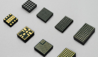
DC-DC Power Modules
Integrated Magnetic Power Module
Buck (Step-Down)-Low Voltage
Buck (Step-Down)-Medium Voltage
Boost (Step-Up)
DC-DC Power Modules
 Magnetically Integrated Power Module (SiP)
Buck (Step-Down)-Multiple Outputs
Buck (Step-Down)
Boost (Step-Up)
Magnetically Integrated Power Module (SiP)
Buck (Step-Down)-Multiple Outputs
Buck (Step-Down)
Boost (Step-Up)
 Customized DC-DC Converters
Tailored Power Modules: Precision Solutions for Your Unique Needs.
Contact Us Today to Discuss Your Project!

DC-DC Power Modules
Customized DC-DC Converters Explore DC-DC Converters
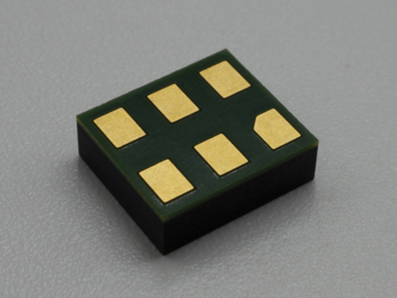
UDM22006 DC DC Integrated Magnetic Power Module ( Input 2.3V–5.5V, output 1.2V-3.3V )
Details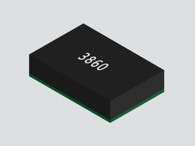
FHT3860 DC/DC Step-Down Buck Power Module ( 2.3V-5.5V Input, 0.5V-3.3V Output )
Details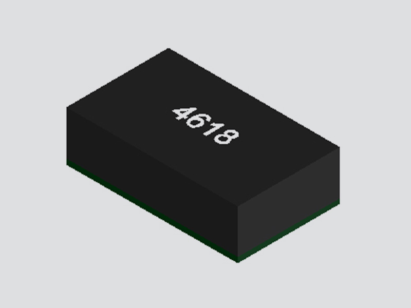
FHT4618 Integrated DC/DC Adjustable Buck Power Module ( 4.5V-24V Input, 0.6V-5.5V Output )
Details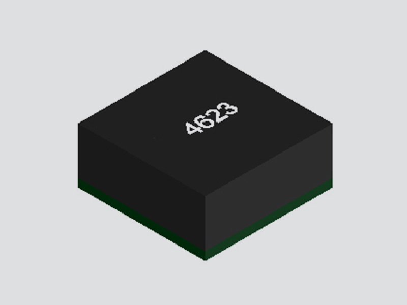
FHT4623 DC/DC Adjustable Buck Converter Power Module ( 4.2V-20V Input, 0.6V-5.5V Output )
Details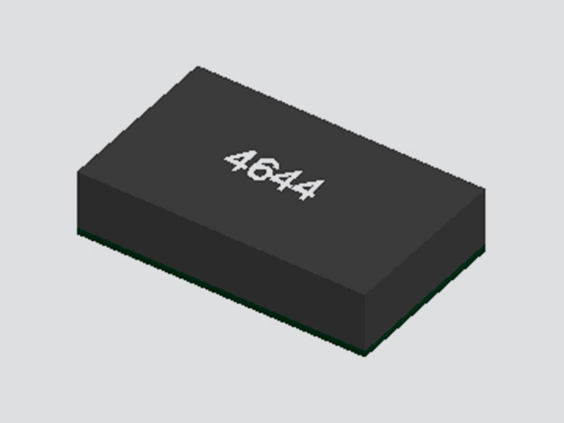
FHT4644 Ultra-Thin Multi-Channel DC/DC Buck Power Module ( 4.0V ~ 15V Input, 0.8V ~ 5.5V Output )
Details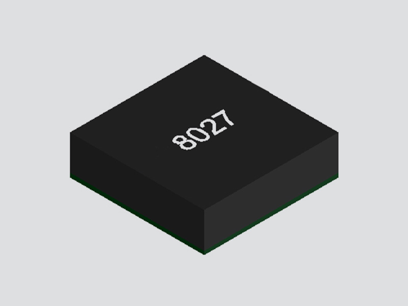
FHT8027C DC/DC Buck Converter Integrated Power Module ( 5V-60V Input, 2.5V-24V Output )
Details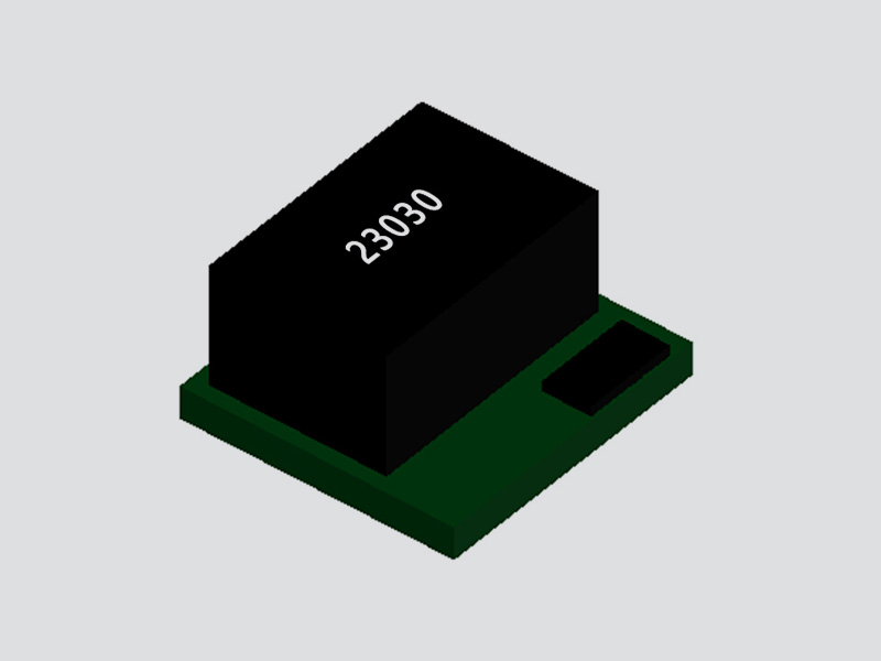
FHT23030 DC/DC Adjustable Buck Converter Module ( 4.5V–17V Input, 0.9V–6V Output )
Details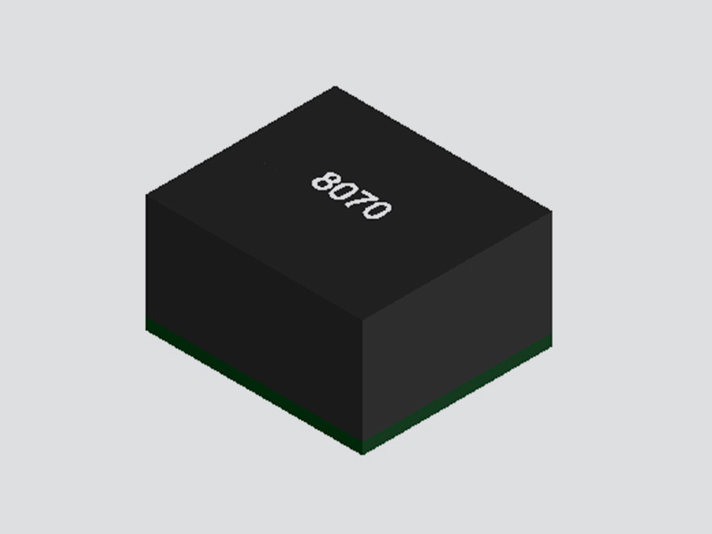
MPPM8070 DC/DC Adjustable Buck Converter Module ( Input 4.5V–18V, Output 0.6V-15V )
Details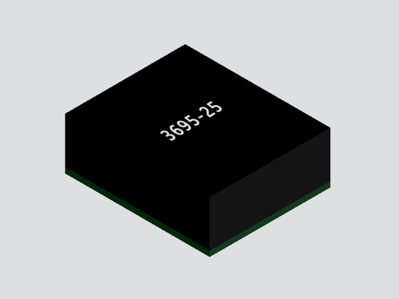
FHM3695 DC/DC Adjustable Buck Power Module ( 4V-16V Input, 0.6V-5.5V Output )
Details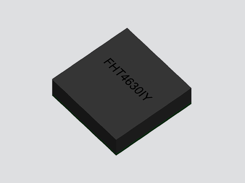
FHT4630 Dual-Channel DC/DC Adjustable Buck Converter Module ( 4.5V~15V Input, 0.6V ~ 1.8V Output )
Details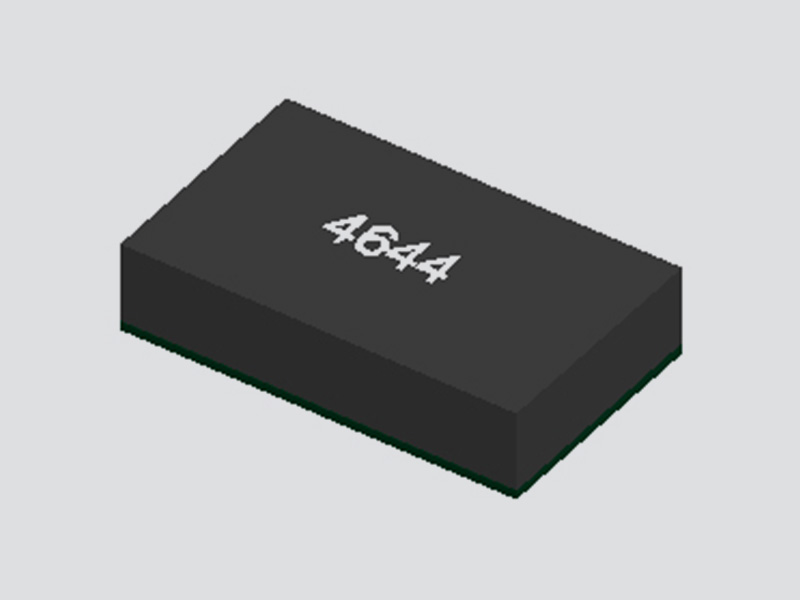
FHT4644C/D 4-Channel DC/DC Buck Power Module with Adjustable Outputs ( 4.5V-14V Input, 0.6V-5.5V Output )
Details
FHT4644F 4-Channel DC/DC Magnetically Integrated Buck Power Module (SiP) | 4.5V to 16V Input, 0.6V to 5.5V Output
Details
FHT4644H 4 Channel Integrated DC/DC Adjustable Buck Power Module ( 4.0V ~ 14V Input, 0.6V ~ 5.5V Output )
Details
FHT4644L 4-Channel Integrated Adjustable Buck DC/DC Power Module ( 4.0V ~ 15V Input, 0.8V ~ 5.5V Output )
Details
UDM2520I Integrated DC/DC Buck Step-Down Power Module ( 2.3V-5.5V Input, 0.8V-3.3V Output )
Details
UDM2826I Integrated DC-DC Buck Step-Down Power Module ( 2.7V-5.5V Input, 1.0V-3.3V Output )
Details
UDM22010 Integrated DC-DC Buck Step-Down Power Module ( 2.3V-5.5V Input, 1.2V-3.3V Output )
Details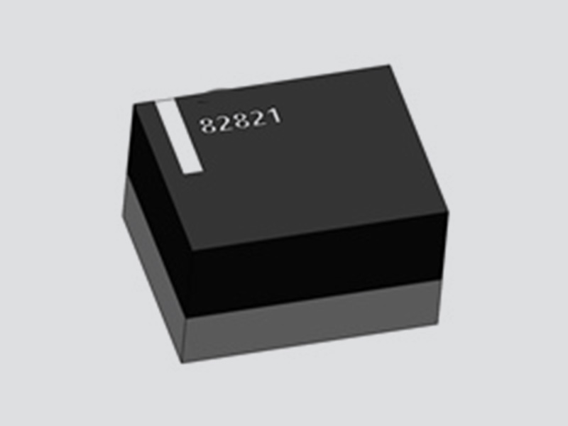
UDM82821 Integrated Magnetic DC-DC Buck Step-Down Power Module ( 2.3V-5.5V Input, 1.2V-3.3V Output )
Details
UDM82821adj Magnetically Integrated DC-DC Buck Power Module ( 2.5V-5.5V Input, 0.8V~4.0V Output )
Details
UDM81256 Integrated DC-DC Boost Power Module ( 2.5V-5.5V Input, Fixed 5V Output )
Details
UDM92403 Integrated DC-DC Boost Step-Up Power Module ( 0.7V-5.5V Input, Adjustable 1.8V-5.5V Output )
Details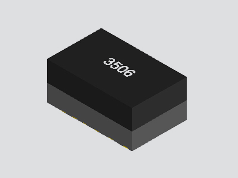
UDM3506 Integrated DC-DC Buck Step-Down Power Converter Module ( 4.7V-36V Input, 0.8V Output )
Details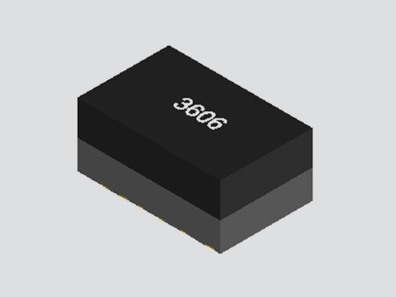
UDM3606 Integrated Medium Voltage DC-DC Buck Step-Down Power Module ( 4.5V-18V Input, 0.6V-5.5V Output )
Details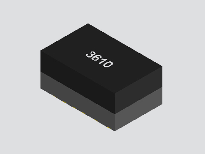
UDM3610 Integrated Medium Voltage DC-DC Buck Step-Down Power Supply Module ( 4.5V-18V Input, 0.6V-5.5V output )
Details5A continuous output current
Wide input voltage range: 3.5V-40V
Output voltage: 1.0V-12.0V
Adjustable switching frequency: 200KHz~2.2MHz
Up to 95% efficiency
Power Good Indicator (PG)
Internal fixed soft start time
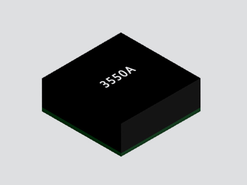
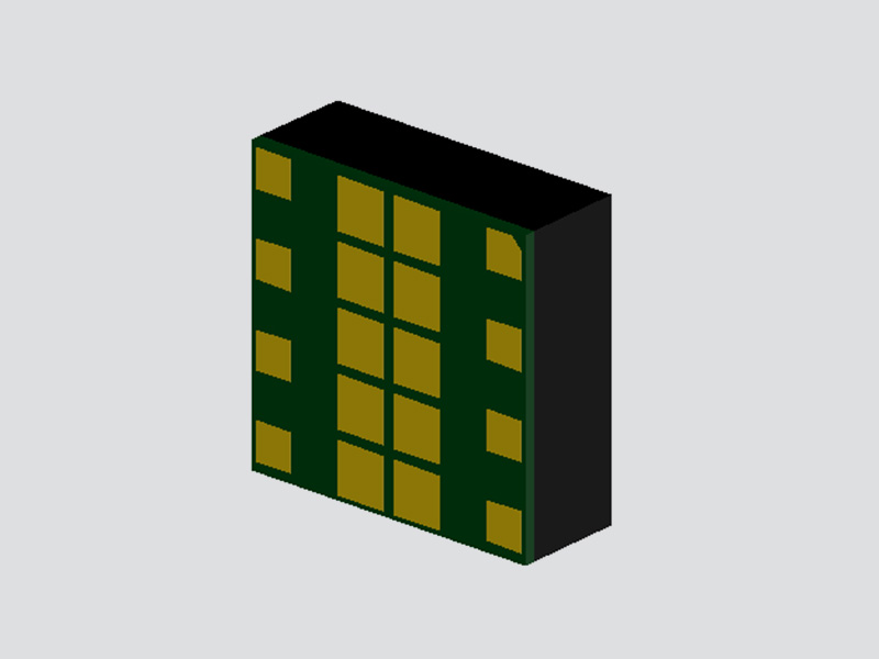
Small size LGA package: (12mm x 12mm x 4.32mm)
Industrial equipment
Telecommunications and network systems
Distribution and POL systems
The FHT3550 is a high-density, non-isolated DC/DC power module suitable for applications with stringent size requirements.
This module offers a highly compact solution with a wide input range and a continuous output current of up to 5A, featuring fast transient response and excellent stability.
The FHT3550 provides an adjustable output voltage of 1.0~12.0V through an external feedback resistor (with a default output of 3.3V) and achieves ultra-high efficiency through the use of synchronous rectification and control technology.
Standard features of the FHT3550 include an internal fixed soft-start function, remote enable control, and a power good indicator. Additionally, the FHT3550 boasts comprehensive protection features, including over-current protection (OCP), short-circuit protection (SCP), input under-voltage lockout protection (UVLO), and over-temperature protection.
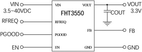
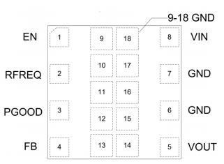
Pin | Symbol | Description |
1 | EN | Enable Pin. Driving EN to a high level turns the module on. Driving EN to a low level turns the module off. |
2 | RFREQ | RFREQ is the input voltage and frequency setting pin connected to the GND pin to determine the on-state period. The RFREQ pin must not be dangled. |
3 | PGOOD | Power Supply Normal Output Indicator Pin. If the output voltage exceeds 90% of the rated voltage, the voltage at the PGOOD pin is pulled high. If the output voltage is less than 85% of the rated voltage, the voltage at the PGOOD pin is pulled low. |
4 |
FB | Voltage Feedback Pin The FHT3550 feedback point voltage is 1 V. For output voltages less than 3.3 V, it is set by connecting an external resistor (RFB1) between the FB pin and the VOUT pin. For applications where the output voltage is greater than 3.3V, the setting is made by connecting an external resistor (RFB2) between the FB pin and GND. |
5 | VOUT | Output Voltage Pin. VOUT is connected inside the module to the internal power inductor and output capacitor. Connect VOUT to the output load and, if desired, connect an external bypass capacitor between VOUT and VIN. |
6, 7, 9-18 | GND | Module Land. |
8 | VIN | The module voltage input pin. vin powers the converter. Connect VIN to the input power supply. If desired, connect an external bypass capacitor between VIN and the GND pin. |
Absolute Maximum Ratings | Conditions | minimum value | nominal value | maximum values | unit (of measure) |
VIN, EN | -0.3 | 42 | V | ||
VOUT | -0.3 | 14 | V | ||
PGOOD | -0.3 | 24 | V | ||
FB,RFREQ | -0.3 | 6 | V | ||
storage temperature | -55 | +150 | ℃ | ||
Input Characteristics | Conditions | minimum value | nominal value | maximum values | unit (of measure) |
Input Voltage Range | 3.5 | 40 | V |
Input current at full load | VIN =36V , VOUT =12V , IOUT =5A | 1.89 | A | ||
Input current at low voltage full load | VIN =5V , VOUT =3.3V , IOUT =5A | 4.05 | A | ||
Input current at no load | VIN =36V , VOUT =12V , IOUT =0A | 0.7 | 1 | mA | |
Input current at shutdown | VIN =36V , VEN =0V | 6 | μA | ||
General Requirements | Conditions | minimum value | nominal value | maximum values | unit (of measure) |
Switching Frequency | Adjusted by RT resistor | 200 | 2200 | KHz | |
Efficiency | 95 | % | |||
Functionality | Conditions | minimum value | nominal value | maximum values | unit (of measure) |
Enable (EN) input turn-on thresholds | Enable Voltage Rise | 1.22 | V | ||
Enable (EN) Input Off Thresholds | Enable Voltage Drop | 1.12 | V | ||
PGOOD Indicator Output Overvoltage Threshold | Output overvoltage | 110 | % | ||
output is normal | 105 | % | |||
PGOOD indication output Undervoltage threshold | Output undervoltage | 90 | % | ||
output is normal | 95 | % | |||
Output Characteristics | Conditions | minimum value | nominal value | maximum values | unit (of measure) |
Output voltage | Adjusted by RFB1 or RFB2 resistor | 1 | 3.3 | 12 | V |
Linear Regulation | VOUT = 3.3V , 5V < VIN < 36V , ILOAD = 5A | ±0.5 | % | ||
Load Regulation | VIN =36V , VOUT =12V,0A < ILOAD ≤ 5A | ±0.8 | % | ||
Output Characteristics | Conditions | minimum value | nominal value | maximum values | unit (of measure) |
Ripple and Noise | VIN =36V , VOUT =12V , IOUT =5A, Cout =22uF ×4, 20MHz bandwidth | 55 | mV | ||
Dynamic Load Response | 50-100% ILOAD , di/dt = 2A/μS; VIN = 36V, VOUT = 12V, And Cout =22uF ×4 |
100 |
mV |
Protective properties | Conditions | minimum value | nominal value | maximum values | unit (of measure) |
Output overvoltage protection | VFB/VREF rising | 110 | % | ||
VFB/VREF drop | 105 | % | |||
Over-temperature shutdown protection | Junction temperature rise | 175 | ℃ | ||
Thermal shutdown hysteresis | 25 | ℃ | |||
Structural Characteristics | Conditions | minimum value | nominal value | maximum values | unit (of measure) |
Size | Length | 11.8 | 12 | 12.2 | mm |
Width | 11.8 | 12 | 12.2 | mm | |
Height | 4.2 | 4.32 | 4.4 | mm | |
Weight | 1 | g | |||
Environmental Adaptability | Conditions | minimum value | nominal value | maximum values | unit (of measure) |
Operating temperature (operating junction temperature) | -40 | 125 | ℃ | ||
High temperature storage (ambient temperature) | +125℃ , 48h | 125 | ℃ | ||
High temperature operation (ambient temperature) | +85°C , 24h; Input low, standard and high pressure for 8h each; VIN =40V , VOUT =12V , IOUT =2.5A |
85 | ℃ | ||
Low temperature storage (ambient temperature) | -55°C, 24h | -55 | ℃ | ||
Low temperature operation (ambient temperature) | -40°C , 24h; Input low pressure, standard pressure, high pressure each 8h | -40 | ℃ | ||
Damp heat | High temperature and high humidity stage: 60℃, 95%; Low temperature and high humidity stage: 30℃, 95%; 10 cycles, each cycle is 24h. |
30 |
60 | ℃ | |
Thermal shock | High temperature 125 ℃, low temperature -55 ℃, high and low temperatures of one hour for a cycle, a total of 32 cycles of the test | -55 | 125 | ℃ |
NOTE 1: Stresses above the values listed in the “Limit Values” section may cause permanent damage to the device. Prolonged exposure to any of the absolute maximum ratings may affect the reliability and life of the device.
Note 2: The maximum continuous output current may be derated due to the FHT3550 junction temperature.
Note 3: The performance specifications of the FHT3550 are guaranteed over the full -40°C to 125°C internal operating stability range. Note that the maximum internal temperature is determined by specific operating conditions in conjunction with the board layout, rated thermal resistance of the package, and other environmental factors.
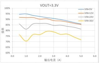
Test conditions are VIN = 24V, VOUT = 3.3V, external COUT = 3x22μF, and TA = 25°C, unless otherwise noted.

Test conditions are VIN = 24V, VOUT = 3.3V, external COUT = 3x22μF, and TA = 25°C, unless otherwise noted.

Test conditions are VIN = 24V, VOUT = 3.3V, external COUT = 3x22μF, and TA = 25°C, unless otherwise noted.

Working Principle
The FHT3550 is a fully integrated synchronous rectifier buck non-isolated switching module. The FHT3550 achieves a continuous output current of 5A over an input voltage range of 3.5V to 40V at an ambient temperature of -40 °C to +125 °C. The FHT3550 provides a default output voltage of 3.3V and is adjustable to 1.0 - 12.0V with an external divider resistor. The FHT3550 provides a default output voltage of 3.3V and can be adjusted to 1.0 - 12.0V with an external divider resistor.
Light load operation mode
Under light load or no load conditions, the FHT3550 will operate in PSM mode to ensure conversion efficiency under these conditions. After the output current exceeds the critical current limit, the switching frequency will be increased over the entire output current range.
Enable Control (EN)
Remote Enable (EN) control utilizes a positive logic that is compatible with today's leading logic devices. Positive logic is defined as enabling the module when the Enable (EN) signal is pulled high and disabling the module when the EN signal is pulled low.
The EN enable control has a typical threshold of 1.22V for rise and 1.12V for fall. The EN pin has a maximum withstand voltage of 42V and can be enabled using VIN or an external voltage enable module.
Note: The enable pin cannot be left dangling.
Internal soft start (SS)
Soft start prevents output voltage overshoot at startup. When the module starts, the internal circuitry generates a soft-start voltage (VSS) that rises slowly at a controlled ramp. When VSS falls below the internal reference (VREF), VSS replaces VREF as the reference for the error amplifier.
Once VSS exceeds VREF, VREF will be used again as the reference value.
At this point, the soft start ends and the FHT3550 enters steady state operation. The soft-start time is set internally to be about 2ms. If VFB drops inexplicably, VSS will follow VFB, which prevents the output voltage from overshooting when a short circuit is recovered. Once the short-circuit is removed, VSS rises slowly like a new soft-start process.
Power Good Output Indication (PGOOD)
The PGOOD pin is an open drain output, and when using the PGOOD indication function, the
A resistor with a resistance between 10kΩ 100kΩ needs to be pulled up to 5V or lower on this pin.
When the FB pin voltage is between 95% and 105% of the internal reference voltage (1V), the PGOOD pin will be open drain. When the FB pin voltage is above 110% or below 90% of the internal reference voltage, the PGOOD pin will be pulled low. In addition, the PGOOD pin will be pulled low when input undervoltage lockout or thermal protection occurs, or when the EN pin is pulled low.
A deviation of the output voltage below 100 µs will not trigger a flip-flop in the PGOOD indication.
Switching Frequency
The FHT3550 operates in PSM mode at no load or light load, and at a set switching frequency when the load reaches a certain value.
The switching frequency can be set by the value of the pull-down resistor from the RFREQ pin to GND (see the "Application Information" section for details).
The switching frequency can be set by the resistance of the pull-down resistor from the RFREQ pin to GND.
The RFREQ resistor is adjustable over a wide range of 200KHz ~ 2.2MHz.
Typical RFREQ pin voltage is 0.5 V. This pin is not allowed to be left open or shorted to ground.
Frequency swing (FSS)
To reduce EMI, the FHT3550 utilizes a switching frequency swing scheme (FSS).
In the vicinity of the set switching frequency, the FSS circuit will oscillate at a certain
The switching frequency is varied by swinging periodically over the frequency range.
Frequency swing
The span is ±6% of the switching frequency and the swing frequency is 1/512 of the switching frequency.
Overcurrent protection (OCP) and short circuit protection (SCP)
The FHT3550 monitors the internal inductor current during the time that the upper or lower to lower switch is energized inside the module.
The FHT3550 utilizes a cycle-by-cycle limiting scheme for the peak current of the upper switches and the valley current of the lower switches to avoid system runaway due to output overloads or short circuits.
Principle of operation
In the event of an output overload or short circuit, the FHT3550 will shut down the output to ensure the safety of the load. When the output voltage falls below the set value due to overcurrent for more than 16 switching cycles, the module will stop operation. After 16.8 ms of stopping, the module will enter soft start again and attempt to reboot into hiccup mode.
In hiccup protection mode, the module will first shut down the outputs, discharge the soft start capacitors, and then attempt to soft start again after a period of time. If the fault condition persists after the soft-start, the module repeats the cycle until the overcurrent/short-circuit condition is eliminated and the output voltage stabilizes at the previous level. By restarting the module at regular intervals, this protection mode significantly reduces the average short-circuit current, mitigates thermal problems, and protects the module.
Overvoltage protection (OVP)
The FHT3550 is designed with output voltage overvoltage protection to minimize output voltage overshoot during load switching, output fault recovery, or light load switching.
The overvoltage comparator compares the FB pin voltage to the internal reference voltage.
When the FB pin voltage exceeds 110% of the internal reference voltage, the system will shut down the upper switch to prevent the output voltage from rising. When the FB pin voltage drops below 105% of the internal reference voltage, the system will resume operation of the upper switch.
Input undervoltage lockout (UVLO) protection
The FHT3550 is designed with an EN enable pin. When the input undervoltage lockout protection function is required, the output voltage VIN can be connected to the EN pin through a resistor divider to realize the input undervoltage lockout (UVLO) protection function by matching the divider voltage value with the EN action threshold.
Over Temperature Shutdown Protection (OTP)
The FHT3550 realizes over-temperature protection by monitoring the junction temperature of the internal IC. This feature allows the module to stop operating at excessive temperatures. If the junction temperature exceeds the threshold value (175 °C), the entire module shuts down. The protection is non-latching. There is a thermal hysteresis of approx. 25 °C. Once the junction temperature has dropped to approx. 150 °C, the module resumes operation via soft start.
Applications Information Output Voltage Setting
The FHT3550 uses an internal feedback resistor divider to set the default output voltage to 3.3 V. The upper voltage divider is 23.2 kΩ and the lower voltage divider is 10 kΩ (see Figure 1).

Fig. 1 Voltage divider resistor for setting output voltage
The FHT3550 regulates its FB voltage to stabilize at 1 V. By connecting an external resistor to the FB pin, the output voltage value can be set from 1 V to 1 V. The output voltage value can be set from 1 V to 1 V by connecting an external resistor to the FB pin.
For applications where VOUT is less than 3.3V, connect FB to the VOUT of the VOUT.
Connect a suitable resistor (RFB1) between the VOUT pins. For applications where VOUT exceeds 3.3V, connect a suitable resistor (RFB2) between the FB and GND pins. Use equations (1) and (2) to roughly calculate the resistance value:

The switching frequency can be adjusted by connecting a resistor between the Rfreq pin and ground. The Rfreq resistor adjusts the switching frequency from 200 kHz to 2.2 MHz, and the Rfreq value is calculated by the following formula (3):

Table 1 shows the relationship between the external resistor values for common operating frequencies.
Table 1 Common Operating Frequencies and Resistance Values

Undervoltage lockout point setting
The FHT3550 supports adjustable input undervoltage lockout (UVLO) with hysteresis through the EN pin divider resistor to achieve application-specific power-up and power-down requirements.

Fig. 2 Undervoltage lockout divider circuit
When the input voltage VIN drops and the voltage divided to the EN pin falls below the
1.12V, the module will stop working. Conversely, as the input voltage, VIN, increases, the voltage across the EN pin rises above 1.22V and the module will begin operation.
The FHT3550 has one 10μF and two 1μF input ceramic capacitors built-in. This is sufficient for common applications. To minimize input voltage ripple, additional external capacitors can be placed next to the VIN pin. The use of low ESR ceramic capacitors helps to achieve optimum performance. Capacitance varies greatly with temperature. X5R and X7R ceramic dielectric capacitors are recommended because of their relatively stable temperature characteristics. Other types of capacitors, such as Y5V and Z5U, are not recommended because they degrade more at frequency, temperature, and bias voltage.
Application information
The ripple current rating of the capacitor must exceed the maximum input ripple current of the converter. The input ripple current can be estimated from equation (4):
 (4)
(4)
The worst case is VIN = 2VOUT.
For simplicity, select an input capacitor with a rated RMS current of more than half the maximum load current.
The capacitance of the input capacitor has a decisive influence on the input voltage ripple of the converter. If there is an input voltage ripple requirement in the application, select an external capacitor that meets the specifications.
Use equation (5) to estimate the input voltage ripple:
 (5)
(5)
Selection of Output Capacitance
The FHT3550 incorporates a 10μF output ceramic capacitor for stabilization. To minimize output ripple and improve load transient response, it is recommended that an external capacitor be added as close to the board as possible.
Low ESR ceramic capacitors are recommended for best performance. Capacitance varies greatly with temperature. X5R or X7R ceramic dielectric capacitors are recommended because of their relatively stable temperature characteristics. Other types of capacitors, such as Y5V and Z5U, are not recommended because they degrade more in capacity at frequency, temperature, and bias voltage. An initial capacitance value of 10 - 47μF can be tried in a single or multiple parallel capacitor configuration. Output voltage ripple can be estimated from equation (6):
 (6)
(6)
When using ceramic capacitors, the impedance at the switching frequency is mainly determined by the capacitance. The output voltage ripple is mainly caused by the capacitance. To simplify the calculation, the output voltage ripple can be estimated by equation (7):
 (7)
(7)
Input Fuse
In general applications, it is necessary to use a fuse at the input of the power module. When there is a possibility of continuous reverse voltage, a fuse should be used instead of a current limiting function. For safety reasons, it is recommended to install a Fast Blow fuse on the ungrounded input power line. The installation application must comply with all relevant safety standards and regulations.
Heat dissipation precautions
Due to its extremely high conversion efficiency and ultra-low power consumption, the FHT3550 can adapt to a very wide range of ambient temperatures. However, if it needs to operate at higher ambient temperatures or provide a large amount of continuous power, it may be necessary to reduce the output current. The current derating should be determined based on the input voltage, output power, and ambient temperature. Refer to the temperature rise curve in the typical performance characteristics section for guidance. Boards of different sizes and layer counts may exhibit different thermal characteristics, which can inconvenience users in verifying correct operation under the system's circuitry, load, and environmental operating conditions. The FHT3550 has an over-temperature shutdown temperature of 175°C, so careful circuit layout is essential to ensure good heat dissipation performance. Most of the heat is dissipated from the bottom layer of the FHT3550 module and the heat sink pad on the PCB. Therefore, poor PCB design can lead to inadequate heat dissipation, thereby reducing the product's performance and reliability.
PCB Layout Guide
The high level of integration of the FHT3550 can reduce or even eliminate PCB layout difficulties. For optimal electrical and thermal performance, good PCB layout is essential. For best results, refer to Figure 3 and follow the guidelines below:
1. For the power layer (VIN, VOUT, and GND), please use large areas of copper pour to minimize conduction losses and thermal stress.
2. Use multiple vias to connect the power board to the inner layers.
Application information
1. Place the vias separately from the pads and vias on the module board. These vias can provide good connections and thermal paths for the internal planes of the PCB.
2. Place ceramic input and output capacitors close to the module pins to minimize high-frequency noise.
3. Use wide and short traces whenever possible. Place the RFB resistor as close as possible to the FB pin.

Figure 3 PCB Layout Reference


Recommended reflow soldering profile

Attention:
1. Due to the large size of the module,please do not place the module under the board for reflow soldering to avoid falling off.

2. For bulk products and those that have been taken out of their original packaging, they should be stored in a desiccator (with a relative humidity of less than 10% inside). For products still in their original packaging, they should also be stored in a desiccator whenever possible.
3.Before mounting on the board, it is necessary to strictly follow the baking conditions to dry the samples: bake at 125°C for more than 48 hours, and control the reflow soldering temperature within 245°C.
| Product Model | Input | Output | Dimensions and Packaging | Packaging | |
| Input Range | Nominal Input | ||||
| FHT3550 | 3.5V~40V | -- | 1V~12V/5A | 12mm × 12mm × 4.32mm (LGA) | Tray |
| Item | Description | Reel/Tray | Pcs/Roll | G.W | N.W | QTY/Carton | Package Size |
FHT3550 | Input 3.5V-40V, output 1.0V-12.0V DC/DC Integrated Plastic Adjustable Buck Power Module, Efficiency up to 95% |
| 500pcs | 1.4kgs | 0.96kgs | 500pcs | 210*210*50mm |
Discover all the technical specifications by downloading the datasheet today.
| Part Number |
Output Current
(A) |
Input Voltage
(V) |
Output Voltage
(V) |
Dimensions(mm) |
Maximum
Efficienc |
Factory Pack
Quantity |
Footprint 3D | Datasheet | Sample |
| UDM2520I | 0.6A | 2.3V ~ 5.5V | 0.8V~3.3V | 2.5mm × 2mm x 1.1mm | 94% | 3,000pcs |  |
 |
|
| UDM22006 | 0.6A | 2.3V~5.5V | 1.2V~3.3V | 2.5mm x 2mm x 1.1mm | 95% | 3,000pcs | |
|
|
| UDM22010 | 1A | 2.3V ~ 5.5V | 1.2V ~ 3.3V | 2.5mm x 2mm x 1.1mm | 95% | 3,000pcs | |
|
|
| UDM82821adj | 1A | 2.5V~5.5V | 0.8V~4V | 2.5mm × 2mm x 1.1mm | 95% | 3,000pcs | |
|
|
| UDM82821 | 1.2A | 2.3V~5.5V | 1.2V~3.3V | 2.5mm × 2mm x 1.1mm | 95% | 3,000pcs | |
|
|
| UDM2826I | 1.5A | 2.7V ~ 5.5V | 1V ~ 3.3V | 2.8mm × 2.6mm x 1.1mm | 93% | 3,000pcs | |
|
|
| UDM3606 | 0.6A | 4.5V-18V | 0.6V-5.5V | 5mm×3.2mm×2.2mm | 95% | 3,000pcs | |
|
|
| UDM3506 | 0.6A | 4.7V-36V | 0.8V | 5mm×3.2mm×2.2mm | 88% | 3,000pcs | |
|
|
| UDM3610 | 1.2A | 4.5V~18V | 0.6V~5.5V | 5mm×3.2mm×2.2mm | 95% | 3,000pcs | |
|
|
| UDM92403 | 0.3A | 0.7V~5.5V | 1.8V~5.5V | 2.5mm×2mm x 1.1mm | 93% | 3,000pcs | |
|
|
| UDM81256 | 1A | 2.5V ~ 5.5V | 5V | 2.8mm×2.6mm×1.35mm(1.1mm) | 95% | 3,000pcs | |
|
|
| FHT4644 | 4A | 4.0V ~ 15V | 0.8V ~ 5.5V | 9mm x 15mm x 4.32mm | 92% | 500pcs | |
|
|
| FHT4644H | 4A | 4.0V ~14V | 0.6V ~ 5.5V | 9mmx15mmx4.32mm | 92% | 500pcs | |
|
|
| FHT4644C/D | 4A | 4.5V-14V | 0.6V-5.5V | 9mmx15mmx4.32mm | 92% | 500pcs | |
|
|
| FHT4644F | 4A | 4.5V ~ 16V | 0.6V ~ 5.5V | 9.0mmx15mmx4.32mm | 92% | 500pcs | |
|
|
| FHT4644L | 4A | 4.0V ~15V | 0.8V ~ 5.5V | 9mmx15mmx1.82mm | 92% | 500pcs | |
|
|
| FHT4630 | 18A+18A | 4.5V~15V | 0.6V ~ 1.8V | 16mm × 16mm × 5.01mm | 94% | 500pcs | |
|
|
| FHT3860 | 6A | 2.3V-5.5V | 0.5V-3.3V | 4mm x 6mm x 1.6mm | 94% | 500pcs | |
|
|
| FHM3695-25 | 20A | 4V-16V | 0.6V-5.5V | 10mm × 12mm ×4.32mm | 95% | 500pcs | |
|
|
| FHT4623 | 3A | 4.2V-20V | 0.6V-5.5V | 6.75mm x 6.75mm x 2.95mm | 95% | 500pcs | |
|
|
| MPPM8070 | 2A | 4.5V-18V | 0.6V-15V | 8mm×7mm × 4.32(2.5mm) | 93% | 500pcs | |
|
|
| FHT4618 | 6A | 4.5V-24V | 0.6V-5.5V | 15mm×9mm×4.32mm | 95% | 500pcs | |
|
|
| FHT23030 | 3A | 4.5V-17V | 0.9V-6V | 3mm×2.8mm×1.4mm | 94% | 500pcs | |
|
|
| FHT3550 | 5A | 3.5V-40V | 1.0V-12.0V | 12mm x 12mm x 4.32mm | 95% | 500pcs | |
|
|
| FHT8027C | 4A | 5V-60V | 2.5V-24V | 15mm×15mm×4.32mm | 95% | 500pcs | |
|

Data Centers and Server Farms

Medical Devices

Aerospace and Defense

Automotive Electronics

Industrial and Automation

Consumer Electronics

Telecommunications and Networking