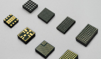


 Integrated Magnetic Power Module
Buck (Step-Down)-Low Voltage
Buck (Step-Down)-Medium Voltage
Boost (Step-Up)
DC-DC Power Modules
Integrated Magnetic Power Module
Buck (Step-Down)-Low Voltage
Buck (Step-Down)-Medium Voltage
Boost (Step-Up)
DC-DC Power Modules
 Magnetically Integrated Power Module (SiP)
Buck (Step-Down)-Multiple Outputs
Buck (Step-Down)
Boost (Step-Up)
Magnetically Integrated Power Module (SiP)
Buck (Step-Down)-Multiple Outputs
Buck (Step-Down)
Boost (Step-Up)
 Customized DC-DC Converters
Tailored Power Modules: Precision Solutions for Your Unique Needs.
Contact Us Today to Discuss Your Project!

DC-DC Power Modules
Customized DC-DC Converters Explore DC-DC Converters
UDM22006 DC DC Integrated Magnetic Power Module ( Input 2.3V–5.5V, output 1.2V-3.3V )
Details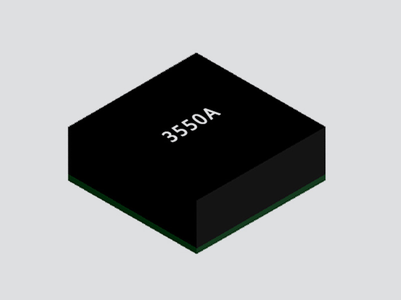
FHT3550 DC/DC Adjustable Buck Power Module ( 3.5V-40V Input, 1.0V-12.0V Output )
Details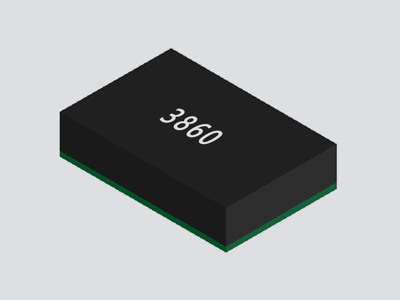
FHT3860 DC/DC Step-Down Buck Power Module ( 2.3V-5.5V Input, 0.5V-3.3V Output )
Details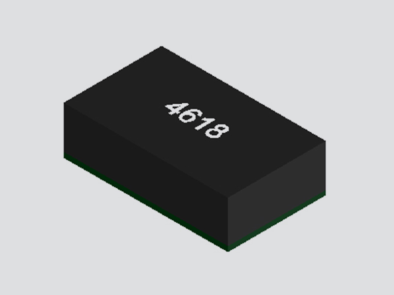
FHT4618 Integrated DC/DC Adjustable Buck Power Module ( 4.5V-24V Input, 0.6V-5.5V Output )
Details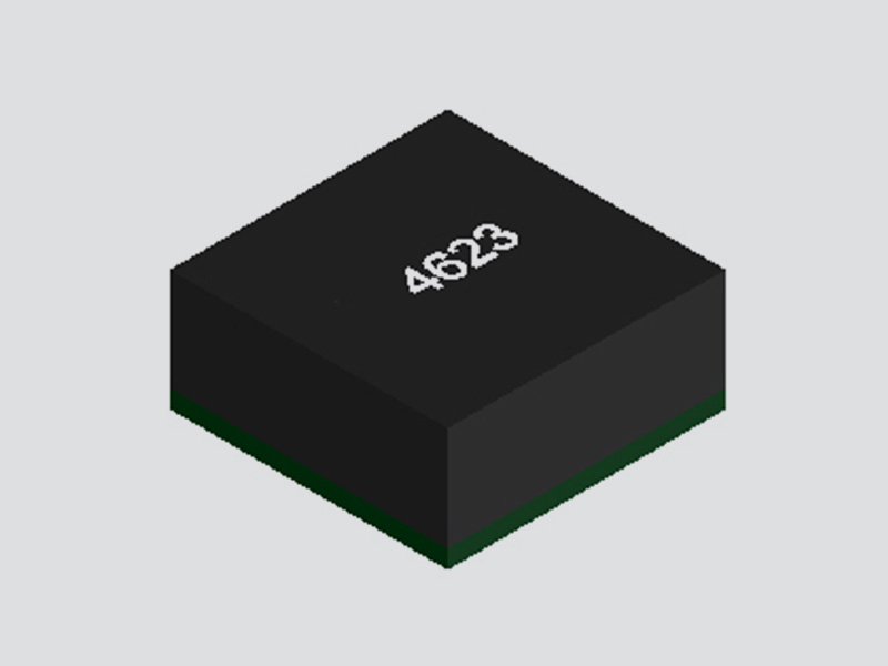
FHT4623 DC/DC Adjustable Buck Converter Power Module ( 4.2V-20V Input, 0.6V-5.5V Output )
Details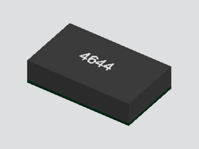
FHT4644 Ultra-Thin Multi-Channel DC/DC Buck Power Module ( 4.0V ~ 15V Input, 0.8V ~ 5.5V Output )
Details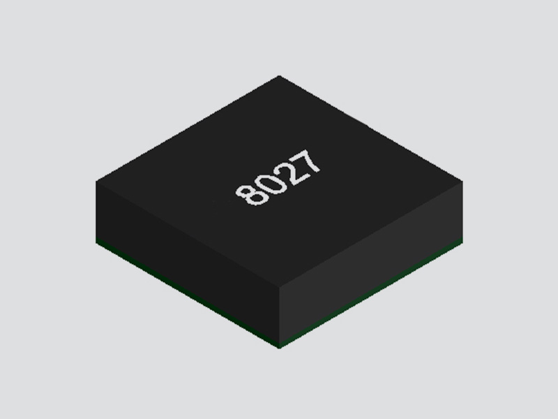
FHT8027C DC/DC Buck Converter Integrated Power Module ( 5V-60V Input, 2.5V-24V Output )
Details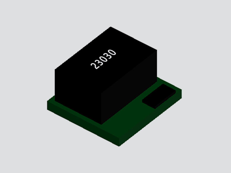
FHT23030 DC/DC Adjustable Buck Converter Module ( 4.5V–17V Input, 0.9V–6V Output )
Details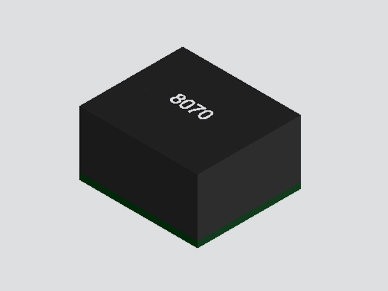
MPPM8070 DC/DC Adjustable Buck Converter Module ( Input 4.5V–18V, Output 0.6V-15V )
Details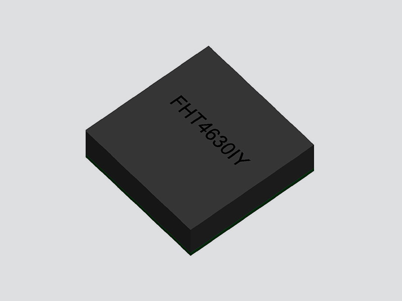
FHT4630 Dual-Channel DC/DC Adjustable Buck Converter Module ( 4.5V~15V Input, 0.6V ~ 1.8V Output )
Details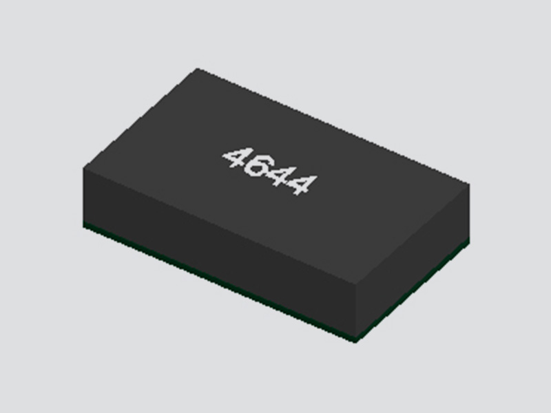
FHT4644C/D 4-Channel DC/DC Buck Power Module with Adjustable Outputs ( 4.5V-14V Input, 0.6V-5.5V Output )
Details
FHT4644F 4-Channel DC/DC Magnetically Integrated Buck Power Module (SiP) | 4.5V to 16V Input, 0.6V to 5.5V Output
Details
FHT4644H 4 Channel Integrated DC/DC Adjustable Buck Power Module ( 4.0V ~ 14V Input, 0.6V ~ 5.5V Output )
Details
FHT4644L 4-Channel Integrated Adjustable Buck DC/DC Power Module ( 4.0V ~ 15V Input, 0.8V ~ 5.5V Output )
Details
UDM2520I Integrated DC/DC Buck Step-Down Power Module ( 2.3V-5.5V Input, 0.8V-3.3V Output )
Details
UDM2826I Integrated DC-DC Buck Step-Down Power Module ( 2.7V-5.5V Input, 1.0V-3.3V Output )
Details
UDM22010 Integrated DC-DC Buck Step-Down Power Module ( 2.3V-5.5V Input, 1.2V-3.3V Output )
Details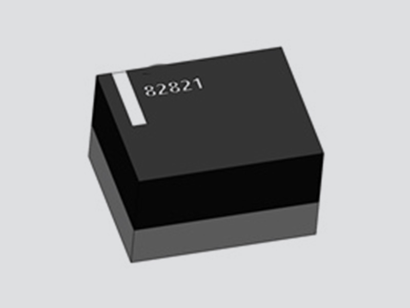
UDM82821 Integrated Magnetic DC-DC Buck Step-Down Power Module ( 2.3V-5.5V Input, 1.2V-3.3V Output )
Details
UDM82821adj Magnetically Integrated DC-DC Buck Power Module ( 2.5V-5.5V Input, 0.8V~4.0V Output )
Details
UDM81256 Integrated DC-DC Boost Power Module ( 2.5V-5.5V Input, Fixed 5V Output )
Details
UDM92403 Integrated DC-DC Boost Step-Up Power Module ( 0.7V-5.5V Input, Adjustable 1.8V-5.5V Output )
Details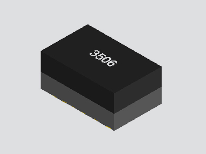
UDM3506 Integrated DC-DC Buck Step-Down Power Converter Module ( 4.7V-36V Input, 0.8V Output )
Details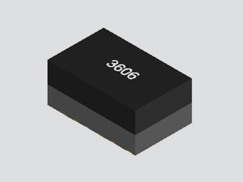
UDM3606 Integrated Medium Voltage DC-DC Buck Step-Down Power Module ( 4.5V-18V Input, 0.6V-5.5V Output )
Details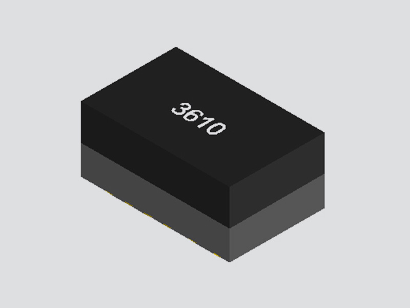
UDM3610 Integrated Medium Voltage DC-DC Buck Step-Down Power Supply Module ( 4.5V-18V Input, 0.6V-5.5V output )
DetailsInput Voltage Range: 4V-16V
Output Voltage: 0.6-5.5V adjustable
Maximum Efficiency: 95%
Rated Output Current: 20A
Maximum Output Current: 25A
Multiphase Parallel Operation: Up to 8 phases can be paralleled, with a maximum paralleled current up to 200A.
Dimensions: 10mm × 12mm ×4.32mm(LGA)
Telecommunications and Networking Systems
Industrial Equipment
Servers and Computing Systems
FPGA/ASIC for AI and Data Mining
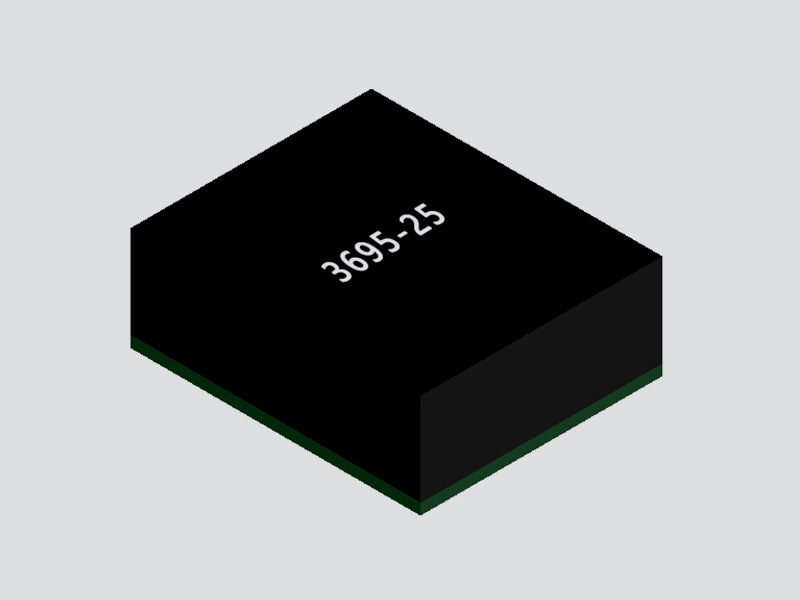
FHM 3695-25 is an expandable, fully integrated, plastic-encapsulated power module with a PMBus interface. FHM 3695-25 offers a complete power supply solution capable of delivering a maximum output current of up to 25A, with excellent load regulation and line regulation. It operates efficiently over a wide load range and can be paralleled to provide higher load currents.
FHM 3695-25 utilizes Multiphase Constant On-Time (MCOT) control, which provides ultra-fast transient response and simple loop compensation. The PMBus interface offers configuration of the module and monitoring of critical parameters.
FHM 3695-25 features comprehensive protection functions, including Over-Current Protection (OCP), Over-Voltage Protection (OVP), Under-Voltage Protection (UVP), and Over-Temperature Protection (OTP). FHM 3695-25 minimizes the use of external components and adopts an LGA-59 (10mm×12mm×4.32mm) package.
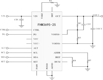
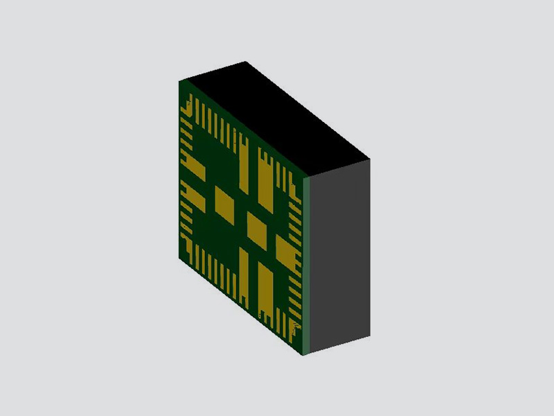
PIN CONFIGURATION
TOP VIEW
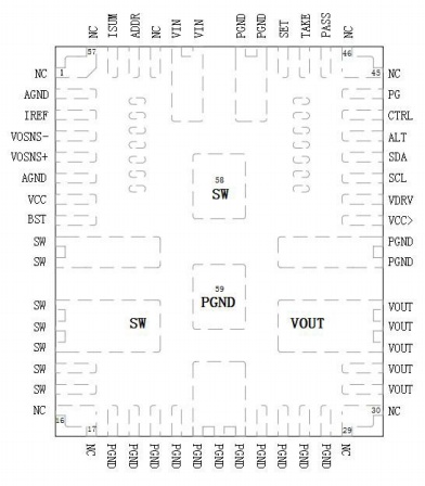
Pin | Symbol | Description |
2,6 | AGND | Signal ground pin. |
3 | IREF | Reference output current pin, keep this pin floating. |
4 | VOSNS- | Output voltage negative sense pin. Connect directly to the GND at the load side. If remote sensing is not used, short it to GND. |
5 | VOSNS+ | Positive output voltage sense pin. Connect this pin to the positive sense point of the output voltage to provide feedback voltage to the system. |
7 | VCC | Output of the internal 5V LDO. |
8 | BST | Bootstrap pin. Floating. |
9-15,58 | SW | Switch output pin. Floating. |
31-35 | VOUT | Module voltage output pin |
18-28,36,37,50,51,59 | PGND | Power ground pin. |
38 | VCC> | Power supply input for the drive circuit. Connect to the VCC pin (pin 7). |
39 | VDRV | Power supply pin for drive and control circuits. Connect a 4.7μF capacitor to ground. |
40 | SCL | PMBus clock pin. |
41 | SDA | PMBus data pin. |
42 | ALT | PMBus alert pin. |
Pin | Symbol | Description |
43 | CTRL | Enable pin. A signal input pin used to turn the module on or off. Connect CTRL to VCC through a pullup resistor. Do not leave this pin floating. |
44 | PG | Output status indication pin. It indicates a high level through a pullup resistor if the output voltage is within the specified range. |
47 | PASS | Voltage loop control signal pin. |
48 | TAKE | Phase address setting pin. Connect a resistor to ground to set the PWM phase. |
49 | SET | Synchronization pin. Connect the SET pins of all modules operating in parallel together to synchronize PWM timing. |
52,53 | VIN | Power supply voltage input pin. |
55 | ADDR | PMBus address setting pin. Connect a resistor between this pin and AGND to set the module's address. |
56 | SUM | Current sharing pin. For single-phase applications, keep this pin floating; for multi-phase applications, connect the ISUM pins of all phases together. |
1,16,17,29, 30,45,46,54,57 | NC | Empty |
Absolute Maximum Ratings | Conditions | Minimum | Nominal | Maximum | Unit |
VIN | 20 | V | |||
VOUT | 5.5 | V | |||
Vcc | -0.3 | 5.5 | V | ||
VSW(DC) | -0.3 | 20 | V | ||
VSW(25ns) | -0.3 | 25 | V | ||
Vbst(DC) | -0.3 | 23.5 | V | ||
All other pins | -0.3 | 5.5 | V | ||
Storage temperature | -55 | +125 | ℃ | ||
Input characteristics | Conditions | Minimum | Nominal | Maximum | Unit |
Input voltage range | 4 | 16 | V | ||
VCC Undervoltage Lockout Threshold (rising) | 2.9 | 3 | 3.1 | V | |
VCC Undervoltage Lockout Threshold (falling) | 2.7 | V |
Input current at full load | VIN=12V,VOUT=5V,IOUT=20A | 8.8 | A | ||
Input current at no load | VIN=12V,VOUT=1.8V,IOUT=0A ,CCM | 60 | mA | ||
Input current when off | ON/OFF=OFF | 2 | 4 | mA | |
Input characteristics | Conditions | Minimum | Nominal | Maximum | Unit |
Switching frequency | 600 | KHz | |||
Efficiency | 95 | % | |||
Functionality | Conditions | Minimum | Nominal | Maximum | Unit |
CTRL enable voltage (rising) | VCC-1 | V | |||
CTRL enable voltage (falling) | 1.2 | V | |||
Soft-start time (tss) | 61h[2:0] = 3b’001 | 2 | m s | ||
Minimum programmable soft-start time (tss_min) | 61h[2:0] = 3b’000 |
1 |
m s | ||
Maximum programmable soft-start time (tss_max) |
16 |
m s | |||
PG high threshold (PGVth Hi Rise) | FB from low to high, default setting (D9h[1:0] = 2b’01) |
0.95 |
VREF | ||
PG low threshold (rise) (PGVth_Lo_Rise) | FB from low to high, default setting (D4h[1:0] = 2b’00) |
1.15 |
VREF | ||
PG low threshold (fall) (PGVth_Lo_Fall) | FB from low to high, default setting (D9h[3:2] = 2b’10) |
0.8 |
VREF |
Characteristics | Conditions | Minimum | Nominal | Maximum | Unit |
Output Voltage | 0.6 | 5.5 | V | ||
Line Regulation | VOUT=3.3V,IOUT=20A | 1.2 | 1.5 | % | |
Load Regulation | VIN=5V,VOUT=3.3V | 2.1 | 2.3 | % | |
Ripple and Noise | VIN=12V,VOUT=1.8V,IOUT=20A | 21 | mV | ||
Dynamic Load Response | 50-100%ILOAD ,di/dt=2.5A/μs | 70 | mV | ||
Output Current Limit (Inductor Valley Current) | D7h = 0x14 | 27 | 30 | 33 A | A |
Structural Characteristics | Conditions | Minimum | Nominal | Maximum | Unit |
Dimensions | 10 × 12 ×4.32 | mm | |||
Weight | 3 | g | |||
Environmental Adaptability | Conditions | Minimum | Nominal | Maximum | Unit |
Operating Temperature (Operating Junction Temperature) | -40 | 125 | ℃ | ||
High Temperature Storage (Ambient Temperature) | +125℃ , 48h | 125 | ℃ | ||
High Temperature Operation (Ambient Temperature) | +85℃ , 24h; Input at low voltage, standard voltage, and high voltage for 8 hours each; VIN =60V ,VOUT =12V ,IOUT=2.4A |
85 | ℃ | ||
Low Temperature Storage (Ambient Temperature) | -55℃ , 24h | -55 | ℃ | ||
Low Temperature Operation (Ambient Temperature) | -40℃ , 24h; Input at low voltage, standard voltage, and high voltage for 8 hours each | -40 | ℃ | ||
Damp Heat | High Temperature and High Humidity Phase:60℃ , 95%; Low Temperature and High Humidity Phase:30℃ , 95%; Cycle for 10 times, with each cycle lasting for 24 hours. |
30 |
60 | ℃ | |
Thermal Shock | High temperature at 125°C and low temperature at -55°C, with each temperature lasting for one hour forming a cycle. The entire test consists of 32 cycles. | -55 | 125 | ℃ |
Note :
Stresses above the values listed in the "Limit Values" section may cause permanent damage to the device. Prolonged exposure to any of the absolute maximum ratings may affect the reliability and lifespan of the device.
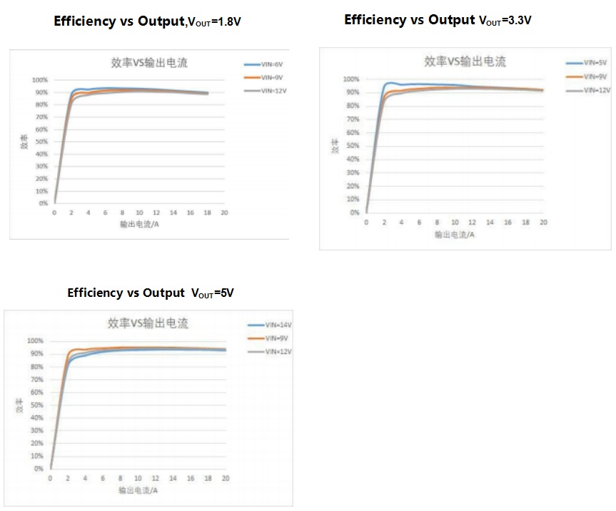
The FHM 3695-25 is a fully integrated power solution that comes in a 10×12×4.32mm LGA package, providing a rated output current of 20A and a peak output current of up to 25A. For applications requiring currents exceeding 25A, parallel connection can be utilized to provide higher output currents.
The FHM 3695-25 employs a Constant On-Time (COT) control method, resulting in fast transient response. Internal slope compensation ensures stable operation in applications using zero ESR ceramic output capacitors.
In a multiphase configuration, one master phase and up to seven slave phases are connected in parallel. All phases equally distribute the output current. A typical application circuit exemplifies the parallel configuration of two FHM 3695-25 devices. In a multiphase setup, the TAKE pin of the master phase needs to be pulled down to ground via a resistor. The FHM 3695-25 detects its master/slave configuration by monitoring the state of the TAKE pin during the startup process.
MCOT Operation - Master Phase
• Receives write and read commands from the host through the PMBus interface
• Generates the SET signal
• Manages startup, shutdown, and all protection operations
• Monitors fault alerts from slave phases via the PG pin
• Generates the first ON pulse
• Generates ON pulses when receiving RUN and SET signals
• Dynamically adjusts its on-time to ensure equal current sharing
The slave phase performs the following functions:
• Receives write commands from the host through the PMBus interface
• Receives the SET signal from the master phase
• Sends OV/UV/OT fault alerts via the PG pin
• Initiates ON pulses when receiving CTRL and SET signals
• Dynamically adjusts its on-time to ensure equal current sharing based on per-phase and total current relative to its own phase
The FHM 3695-25 benefits from MCOT control, enabling extremely fast load transient response. During load transients, SET signals are generated more frequently compared to steady-state conditions. Therefore, energy is delivered to the load at a higher rate, minimizing output deviation during load transients. For the FHM 3695-25, SET pulses are generated with a minimum interval of 50ns, meaning that the next phase can be turned on as quickly as 50ns after the previous one.
Multiphase Parallel Phase Configuration
When applying the FHM3695 in a multiphase parallel configuration, phase configuration needs to be achieved by connecting a corresponding resistance value from the ADDPH pin to ground, thereby enabling phase staggering and equal current sharing.
Phase Sequence | R_ADDPH(kΩ) |
1 | 5 |
2 | 15 |
3 | 25 |
4 | 37 |
5 | 52 |
6 | 70 |
7 | 95 |
8 | 125 |
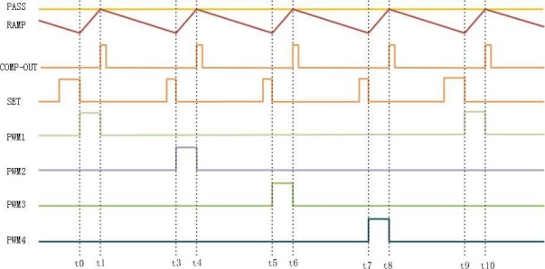
Four-Phase Operating Timing Diagram (Steady State)
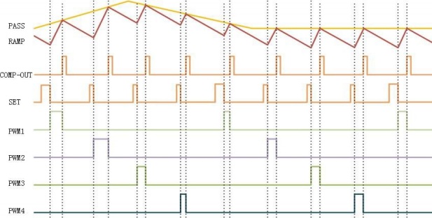
Four-Phase Operating Timing Diagram (Dynamic State)
Working Mode Selection
The FHM 3695-25 offers a forced CCM (Constant Current Mode) and frequency hopping working mode under light load conditions, which can be set via PMBus with commands as shown in Table
Table 1 MFR_CTRL_OPS(D2h)
Bits | Name | Default | Description |
[7:3] | Reserved | 00000 | |
[0] | SKIP_CCM | 1 | 0: Frequency Hopping Mode 1: Forced CCM Mode |
Operating Frequency
The operating frequency of the FHM 3695-25 is 600KHz.
Output Voltage Setting
The output voltage of the module can be set by the pullup resistor RTOP between VOSNS+ and VOUT, and the pulldown resistor RBOTTOM between VOSNS+ and VOSNS-. The reference calculation formula is as follows:
Soft Start
The soft start (SS) time can be programmed via PMBus. The default time is 2ms.
Pre-Bias Start-Up
The FHM 3695-25 ensures a monotonic rising start-up when the output voltage is biased. If the output voltage is pre-biased to a certain voltage during start-up, both the high-side and low-side switches will be disabled until the sensed output voltage on the VOSNS+ pin falls below the internal reference voltage.
Current Sensing and Over-Current Protection (OCP)
The FHM3695-25 features on-chip current sensing and a programmable positive current limit threshold.
The FHM 3695-25 provides two inductor valley current limits (set by register D7h).
Inductor Valley Over-Current Protection (D7h)
During the LS-FET conduction state, the inductor current is sensed and monitored on a cycle-by-cycle basis. The HS-FET is only allowed to conduct if no over-current is detected during the LS-FET conduction state. If 31 consecutive OC conditions are detected, the OCP is triggered.
In the case of an over-current condition or output short-circuit, if the output voltage falls below the Under-Voltage Protection (UVP) threshold, the FHM 3695-25 immediately enters over-current protection mode.
After triggering the OCP, whether the FHM3695-25 enters hiccup mode or latch-off mode depends on the register settings. It should be noted that once latched off, re-enabling the FHM 3695-25 requires restarting Vcc or CTRL.
The inductor valley over-current limit can be programmed via register D7h, which sets the inductor valley current limit for each phase for both single-phase and multi-phase operations. The commands are shown in Table 3.
Table3 MFR_OC_PHASE_SET(D7h)
Bits | Name | Default | Description |
[7:5] | Reserved | 000 | |
[4:0] | OC_limit | 10100 | Current Limit。 1.5A/LSB, [00000] = 0A。 |
Negative Phase Inductor Current Limit
When the current sensed by the LS-FET falls below the negative phase current limit set by register D5h[2], the device will turn off its LS-FET for a period of time to limit the load current. The period can be set via register D5h[3]. The commands are shown in Table 4.
Table4 MFR_OVP_NOCP_SET (D5h)
Bits | Name | Default | Description |
[7:4] | Reserved | 0000 | |
[3] | DELAY_NOCP(D400) | 0 | 0: 100ns delay after NOCP 1:200ns delay after NOCP |
[2] |
NOCP |
0 | 0: Set NOCP to -10A 1: Set NOCP to -15A |
Over-Voltage Protection (OVP)
The FHM 3695-25 monitors the output voltage via the VOSNS+ pin at the resistor divider to detect over-voltage conditions. The over-voltage protection value can be set via register D4h, with specific commands shown in Table 5.
Table5 MFR_VOUT_OVP_FAULT_LIMIT (D4h)
Bits | Name | Default | Description |
[7:4] | Reserved | 0000 | |
[3:2] |
OV_EXIT_TH |
00 | Set the exit threshold for OVP 00: 10% * VREF 01: 50% * VREF 10: 80% * VREF 11: 102.5% * VREF |
[1:0] |
OV_ENTRY_TH |
00 | Set the entry threshold for OVP 00: 115% *VREF 01: 120% *VREF 10: 125% *VREF 11: 130% *VREF |
Under-Voltage Protection (UVP)
The FHM 3695-25 monitors the output voltage through the VOSNS+ pin to detect under-voltage conditions. If the VOSNS+
voltage falls below the UVP threshold (set via register D9h, as shown in Table 6), the UVP is triggered. Upon triggering the UVP, the FHM 3695-25 will enter either HICCUP mode or latch-off mode, depending on the PMBus configuration. Please note that once the device is latched off, to re-enable the FHM 3695-25, a restart of Vcc or CTRL is required.
Table 6 MFR_UVP_PGOOD_ON_LIMIT (D9h)
Bits | Name | Default | Description |
[7:4] | Reserved | 0000 | |
[3:2] |
UV_TH |
00 | Set the UVP threshold. When the FB voltage drops below the UV_TH level, UVP is triggered. 00: 69% * VREF 01: 74% * VREF 10: 79% * VREF 11: 84% * VREF |
Output Sink Mode (OSM)
When the output voltage exceeds the reference voltage by more than 5% but remains below the OVP threshold, the FHM 3695-25 enters OSM. Upon triggering OSM, the FHM 3695-25 operates in forced CCM mode. The FHM 3695-25 exits OSM mode when the HS-FET is re-activated. This feature can be enabled or disabled via register EAh[9], with instructions provided in Table 7.
Table 7 MFR_CTRL(EAh)
Bits | Name | Default | Description |
[15:1 1] | Reserved | 00000 | |
[9] |
OSM |
0 | Enable or Disable OSM Function. 0: Enable 1: Disable |
Over-Temperature Protection (OTP)
The FHM 3695-25 monitors the junction temperature. If the junction temperature exceeds the threshold, the converter will enter either HICCUP mode or latch-off mode, depending on the PMBus selection. Please note that once latched off, to re-enable the MPM3695-25 (assuming it's a typo for FHM 3695-25), a restart of Vcc or CTRL is required.
The junction temperature threshold can be set via register 4Fh, with specific instructions provided in Table 8. The value is unsigned, with 1 LSB equaling 1 °C, and the default value is 0x009B (155 °C).
Table 8 OT_FAULT_LIMIT (4Fh)
Bit | 15 | 14 | 13 | 12 | 11 | 10 | 9 | 8 |
Access | r | |||||||
Function | C/LSB | |||||||
Default value | 0 | 0 | 0 | 0 | 0 | 0 | 0 | 0 |
Bit | 7 | 6 | 5 | 4 | 3 | 2 | 1 | 0 |
Access | r/w | |||||||
Function | C/LSB | |||||||
Default value | 1 | 0 | 0 | 1 | 1 | 0 | 1 | 1 |
Power Good(PG)
The FHM 3695-25 features an open-drain signal pin for determining power good (PG) status. The PG pin can be configured as an output-only pin or as both an input and output pin via bit [0] of the MRF_CTRL_COMP (D0h) register, as shown in Instruction Table 9. For single-phase configurations, the PG pin should be configured solely as an output pin. For multi-phase operations, the PG pin should be configured as both an input and output pin to detect faults in the phases. It is necessary to pull the PG pin up to VCC or the voltage source through a pull-up resistor (typically 100kΩ).
Once input voltage is applied to the FHM 3695-25, the PG pin is pulled low. When the VOSNS+ voltage reaches the threshold set in register D9h (as shown in Instruction Table 10) and after the delay set in register D1h (as shown in Instruction Table 11), the PG pin is pulled high.
In the event of any fault, the PG pin latches low and triggers related protection functions (such as UV, OV, OT, UVLO, etc.). Once the PG pin is latched low, it cannot be pulled high again unless a new soft start is initiated.
Table 9 MFR_CTRL_COMP (D0h)
Bits | Name | Default | Description |
[7:5] | Reserved | 0000 | |
[0] | Slave Fault Detection | 1 | 0: Enable phase fault detection 1: Disable from phase fault detection |
Table 10 MFR_UVP_PGOOD_ON_LIMIT (D9h)
Bits | Name | Default | Description |
[7:4] | Reserved | 0000 | |
[1:0] |
PG_ON |
00 | Set the FB threshold for PG to be pulled high during soft start. Once the FB reaches the threshold, the PG will be pulled high after a delay set by D1[5:2]. 00: 90% * VREF 01: 92.5% * VREF 10: 95% * VREF 11: 97.5% * VREF |
Table 11 MFR_CTRL_VOUT (D1h)
Bits | Name | Default | Description |
[7] | Reserved | 0 | |
[5:2] | PG delay |
0000 | Set the PG pull-up time after the soft start is completed. |
Bits | Name | Default | Description |
[7:5] | Reserved | 0000 | |
[0] | Slave Fault Detection | 1 | 0: Enable phase fault detection 1: Disable from phase fault detection |
Layout
The layout of the PCB is crucial for the stability of the power module's operation. To achieve optimal performance, please follow these guidelines:
1. Place the input ceramic capacitors as close as possible to the VIN and PGND pins. Use large copper pours for VIN and PGND to minimize parasitic impedance and reduce thermal resistance.
2. Add VIN vias at least 3mm away from the device to minimize noise coupling caused by input pulse currents.
3. Connect AGND and PGND at a single point.
4. Place sufficient output PGND vias near the PGND pin to minimize parasitic impedance and thermal resistance.
5. Keep the ISUM trace as short as possible. In multi-phase configurations, the ISUM trace should be kept away from the VIN copper pour area. Avoid using vias as much as possible.
6. Avoid routing signal traces directly under the SW pads unless the PGND layer is used to provide shielding.
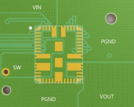
Recommended PCB Layout
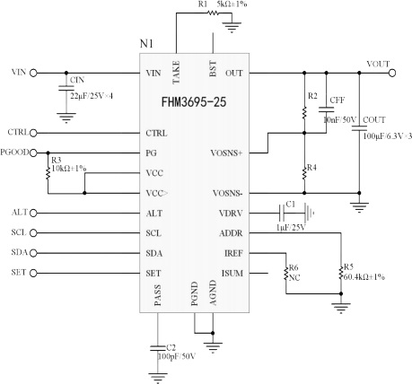
Typical Circuit: Single-Phase Application
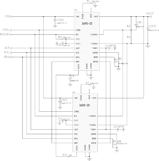
Typical Circuit: Two-Phase Parallel Application
PMBUS Serial Interface
PMBus Serial Interface Explanation
The Power Management Bus (PMBus) is a two-wire, bidirectional serial interface comprising a data line (SDA) and a clock line (SCL). When the lines are "idle," they are pulled up to the bus voltage by an external source. When connected to the lines, the master device generates the
SCL signal and the device address, and orchestrates the communication sequence.
It operates based on I2C principles. The FHM 3695-25 interface serves as a PMBus slave, supporting both standard mode (100kHz) and fast modes (400kHz and 1MHz). The PMBus interface adds flexibility to power supply solutions.
Device Address
To manage multiple FHM 3695-25 devices through the same PMBus, please use the ADDR pin to program the device address for each FHM 3695-25. The ADDR pin has a current outflow of 10μA. Connect a resistor between the ADDR pin and AGND to set the ADDR voltage. The PMBus address is set by converting the pin voltage using an internal ADC. The ADDR pin can set up to 16 unique addresses. Additionally, the MFR_ADDR_PMBUS (D3h) register can be used to set the PMBus address digitally.
Once an address is selected, each device must
have a unique address during normal operation.
Table 12 shows the relationship between ADDR resistor values and PMBus addresses.
Tbale12 PMBUS Address Setting
Table 12 PMBUS
R_ADD T(kΩ) | Slave Address (R_ISET=60.4kΩ) | Slave Address (R_ISET=180kΩ) |
5 | 30h | 40h |
15 | 31h | 41h |
25 | 32h | 42h |
37 | 33h | 43h |
52 | 34h | 44h |
70 | 35h | 45h |
95 | 36h | 46h |
125 | 37h | 47h |
Start and Stop Conditions
The master device initiates START/STOP signals to indicate the beginning and end of PMBus data transmission. The START condition is defined as the SDA signal transitioning from high to low while SCL is high. The STOP condition is defined as the SDA signal transitioning from low to high while SCL is high.
The master device generates the SCL clock and sends the device address and read/write direction bit R/W on the SDA line. Data is transmitted on the SDA line in 8-bit bytes. Each data byte is followed by an acknowledge bit.
PMBus Update Timing
When updating the FHM 3695-25, it requires a start condition, a valid PMBus address, a register address byte, and data bytes for a single packet update. After receiving each byte, the FHM 3695-25 acknowledges by pulling the SDA line low during the high level of a single clock pulse. A valid PMBus address selects the FHM 3695-25 for communication. The FHM 3695-25 performs the update on the falling edge of the LSB (least significant byte) byte.
Packet Error Checking (PEC)
The FHM 3695-25 PMBus interface supports the use of a Packet Error Checking (PEC) byte. The PEC byte is either sent by the FHM 3695-25 during a read operation or transmitted by the bus master to the FHM 3695-25 during a write operation.
The bus master or the FHM 3695-25 uses the PEC byte to detect errors during bus communication, depending on whether it is a read or write operation. If the master determines that the PEC byte read during a read operation is incorrect, it can decide to retry the read. If the FHM 3695-25 determines that the PEC byte sent during a write operation is incorrect, it ignores the command (does not execute it) and sets a status flag. In group commands, the master can choose to send or not send a PEC byte as part of the message to the FHM 3695-25.
PMBus Alarm Response Address (ARA)
The PMBus Alarm Response Address (ARA) is a special address that the bus master can use to locate any device that needs to communicate with it. The master typically uses hardware interrupt pins to monitor the PMBus ALERT pins of many devices. When the master is interrupted, it sends a message on the bus using PMBus receive bytes or bytes received with the PEC protocol.
The special address used by the master is 0x0C. Any device with a PMBus alert signal returns its own 7-bit address as the 7 most significant bits (MSBs) of a data byte. The least significant bit (LSB) is not used and can be either 1 or 0. The master reads the device address from the received data byte and then proceeds to handle the alert condition.
Multiple devices may have a valid PMBus alert signal and attempt to communicate with the master. In this case, the device with the lowest address takes control of the bus and successfully sends its address to the master. The successful device then disables its PMBus alert signal. If the master finds that the PMBus alert signal remains low, it will continue to read addresses until all devices that need to communicate with it have successfully sent their addresses
OPERATION (01h)
The OPERATION is a paged register. The OPERATION command is used to turn the converter's output on/off and to control the input of the CTRL pin. It is also used to set the upper or lower limit of the output voltage. The unit remains in the commanded mode until a subsequent OPERATION command or a change in the CTRL pin state instructs the converter to switch to another mode. This OPERATION command is also used to re-enable the converter after it has been shut down due to a fault trigger. Writing an OFF command after an ON command will clear all faults. However, simply writing an ON command after a fault-triggered shutdown will not clear the fault registers. The default value is 0x80.
Command | OPERATION | |||||||
Format | Unsigned binay | |||||||
Bit | 7 | 6 | 5 | 4 | 3 | 2 | 1 | 0 |
Access | r/w | r/w | r/w | r/w | r/w | r/w | r/w | r/w |
Function | x | x | ||||||
Default value | 1 | 0 | 0 | 0 | 0 | 0 | x | x |
Bit[7:6] | Bit[5:4] | Bit[3:2] | Bit[1:0] | On/off | Margin state | 01h |
00 | xx | xx | xx | Immediate off | N/A | 0x00 |
01 | xx | xx | xx | Immediate off | N/A | 0x60 |
10 | 00 | xx | xx | on | off | 0x80 |
10 | 01 | 01 | xx | on | Margin low (ignore fault) | 0x94 |
10 | 01 | 10 | xx | on | Margin low (act on fault) | 0x98 |
10 | 10 | 01 | xx | on | Margin high (ignore fault) | 0xA4 |
10 | 10 | 10 | xx | on | Margin high (act on fault) | 0xA8 |
ON_OFF_CONFIG (02h)
The ON_OFF_CONFIG command configures the CTRL pin input and sets the combination of PMBus commands required to turn the converter on and off. The default value for this command is 0x16.
Command | OPERATION | |||||||
Format | Unsigned binay | |||||||
Bit | 7 | 6 | 5 | 4 | 3 | 2 | 1 | 0 |
Access | r | r | r | r/w | r/w | r/w | r/w | r/w |
Function | X | X | X | on | op | ctrl | pol_ctrl | delay |
Default value | 0 | 0 | 0 | 1 | 0 | 1 | 1 | 1 |
CLEAR_FAULTS (03h)
The CLEAR_FAULTS command is used to reset all stored warning and fault flags.
CAPABILITY (19h)
The CAPABILITY command returns information about the PMBus features supported by the FHM 3695-25. This command is read using the PMBus read-byte protocol. The default value for this command is 0xB0.
Command | CAPABILITY | |||||||
Format | Unsigned binay | |||||||
Bit | 7 | 6 | 5 | 4 | 3 | 2 | 1 | 0 |
Access | r | r | r | r | r | r | r | r |
Function | PEC | Max.bus speed | Alert | x | x | x | x | |
Default value | 1 | 0 | 1 | 1 | 0 | 0 | 0 | 0 |
PEC supported, max speed 1MHz, supports PMBusTM alert and ARA. | ||||||||
Bit[6:5] | Meaning | |
0 | 0 | Maximum supported bus speed is 100kHz. |
0 | 1 | Maximum supported bus speed is 1MHz. |
1 | 0 | Maximum supported bus speed is 400kHz. |
1 | 1 | Reserved. |
VOUT_MODE (20h)
The VOUT_MODE command is used to command and read the output voltage. The three most significant bits are used to determine the data format (with the FHM 3695-25 only supporting the direct format), and the remaining five bits represent the exponent used in the output voltage read/write commands. The default value for this command is 0x40.
VOUT_COMMAND (21h)
The VOUT_COMMAND sets the output voltage of the FHM 3695-25. The value is unsigned and has a resolution of 1 LSB = 2 mV. The default value for this command is 0x0258, which corresponds to 1.2V.
Command | VOUT_COMMAND | |||||||||||||||
Format | Direct | |||||||||||||||
Bit | 15 | 14 | 13 | 12 | 11 | 10 | 9 | 8 | 7 | 6 | 5 | 4 | 3 | 2 | 1 | 0 |
Access | r | r | r | r | r/w | r/w | r/w | r/w | r/w | r/w | r/w | r/w | r/w | r/w | r/w | r/w |
Function | X | |||||||||||||||
Default value | 0 | 0 | 0 | 0 | 0 | 0 | 1 | 0 | 0 | 1 | 0 | 1 | 1 | 0 | 0 | 0 |
VOUT_MAX (24h)
The VOUT_MAX command sets the upper limit of the converter's output voltage, regardless of any other commands or combinations. The purpose of this command is to prevent users from accidentally setting the output voltage to an excessively high level that exceeds the device's maximum voltage tolerance, not just the overvoltage protection range. The value is unsigned and has a resolution of 1 LSB = 2 mV. The default value for this command is 0x0ABE, which corresponds to 5.5V.
Command | VOUT_MAX | |||||||||||||||
Format | Direct | |||||||||||||||
Bit | 15 | 14 | 13 | 12 | 11 | 10 | 9 | 8 | 7 | 6 | 5 | 4 | 3 | 2 | 1 | 0 |
Access | r | r | r | r | r/w | r/w | r/w | r/w | r/w | r/w | r/w | r/w | r/w | r/w | r/w | r/w |
Function | X |
VOUT_SCALE_LOOP (29h)
The VOUT_SCALE_LOOP sets the feedback resistor divider ratio, which is equal to VOSNS+/VOUT. Regardless of whether an external or internal feedback resistor divider is used, VOUT_SCALE_LOOP should match the actual feedback resistor divider that is being utilized. The value is unsigned and has a resolution of 1 LSB = 0.001. The default value for this command is 0x01F4, which corresponds to 0.5.
OT_FAULT_LIMIT (4Fh)
OT_FAULT_LIMIT (4Fh)
The OT_FAULT_LIMIT command is used to configure or read the threshold for over-temperature fault detection. If the measured temperature exceeds this value, over-temperature protection will be triggered. The value is unsigned and has a resolution of 1 LSB = 1°C. The default value for this command is 0x009B, which corresponds to 155°C.
Command | OT_FAULT_LIMIT | |||||||||||||||
Format | Direct | |||||||||||||||
Bit | 15 | 14 | 13 | 12 | 11 | 10 | 9 | 8 | 7 | 6 | 5 | 4 | 3 | 2 | 1 | 0 |
Access | r | r | r | r | r | r | r | r | r/w | r/w | r/w | r/w | r/w | r/w | r/w | r/w |
Function | X | 1。C/LSB | ||||||||||||||
Default value | 0 | 0 | 0 | 0 | 0 | 0 | 0 | 0 | 1 | 0 | 0 | 1 | 1 | 0 | 1 | 1 |
OT_WARN_LIMIT (51h)
The OT_WARN_LIMIT is used to configure or read the threshold for over-temperature warning detection. The value is unsigned and has a resolution of 1 LSB = 1°C. The default value for this command is 0x0091, which corresponds to 145°C.
Command | OT_WARN_LIMIT | |||||||||||||||
Format | Direct | |||||||||||||||
Bit | 15 | 14 | 13 | 12 | 11 | 10 | 9 | 8 | 7 | 6 | 5 | 4 | 3 | 2 | 1 | 0 |
Access | r | r | r | r | r | r | r | r | r/w | r/w | r/w | r/w | r/w | r/w | r/w | r/w |
Function | X | 1。C/LSB | ||||||||||||||
Default value | 0 | 0 | 0 | 0 | 0 | 0 | 0 | 0 | 1 | 0 | 0 | 1 | 1 | 0 | 0 | 1 |
VIN_OV_FAULT_LIMIT (55h)
The VIN_OV_FAULT_LIMIT command is used to configure or read the threshold for input over-voltage fault detection. The value is unsigned and has a resolution of 1 LSB = 500 mV. The default value for this command is 0x0021, which corresponds to 16.5V. The set value should not exceed 18V.
Command | VIN_OV_FAULT_LIMIT | |||||||||||||||
Format | Direct | |||||||||||||||
Bit | 15 | 14 | 13 | 12 | 11 | 10 | 9 | 8 | 7 | 6 | 5 | 4 | 3 | 2 | 1 | 0 |
Access | r | r | r | r | r/w | r/w | r/w | r/w | r/w | r/w | r/w | r/w | r/w | r/w | r/w | r/w |
Function | x | 500mV/LSB | ||||||||||||||
Default value | 0 | 0 | 0 | 0 | 0 | 0 | 0 | 0 | 0 | 0 | 1 | 0 | 0 | 0 | 0 | 1 |
VIN_OV_WARN_LIMIT (57h)
The VIN_OV_WARN_LIMIT command is used to configure or read the threshold for input over-voltage warning detection. The value is unsigned and has a resolution of 1 LSB = 500 mV. The default value for this command is 0x0021, which corresponds to 16.5V. The maximum value should not exceed 18V.
Command | VIN_OV_WARN_LIMIT | |||||||||||||||
Format | Direct | |||||||||||||||
Bit | 15 | 14 | 13 | 12 | 11 | 10 | 9 | 8 | 7 | 6 | 5 | 4 | 3 | 2 | 1 | 0 |
Access | r | r | r | r | r/w | r/w | r/w | r/w | r/w | r/w | r/w | r/w | r/w | r/w | r/w | r/w |
Function | x | 500mV/LSB | ||||||||||||||
Default value | 0 | 0 | 0 | 0 | 0 | 0 | 0 | 0 | 0 | 0 | 1 | 0 | 0 | 0 | 0 | 1 |
VIN_UV_WARN_LIMIT (58h)
The VIN_UV_WARN_LIMIT command is used to configure or read the threshold for input under-voltage warning detection. The value is unsigned and has a resolution of 1 LSB = 250 mV. The default value for this command is 0x0010, which corresponds to 4V. The minimum value should not be less than 3.3V.
Command | VIN_UV_WARN_LIMIT | |||||||||||||||
Format |
Direct | |||||||||||||||
Bit | 15 | 14 | 13 | 12 | 11 | 10 | 9 | 8 | 7 | 6 | 5 | 4 | 3 | 2 | 1 | 0 |
Access | r | r | r | r | r/w | r/w | r/w | r/w | r/w | r/w | r/w | r/w | r/w | r/w | r/w | r/w |
Function | x | 250mV/LSB | ||||||||||||||
Default value | 0 | 0 | 0 | 0 | 0 | 0 | 0 | 0 | 0 | 0 | 1 | 0 | 0 | 0 | 0 | 0 |
TON_DELAY (60h)
This command is read-only, and the default value is 0x0000 (0ms).
TON_RISE (61h)
The TON_RISE command sets the soft-start time, in milliseconds, which refers to the time it takes for the output to rise from the start until the voltage reaches its regulated point. The value is unsigned, with 1 LSB = 1 ms. The default value is 0x0001 (2 ms), and the maximum value is 0x0007 (16 ms).
Command | TON_RISE | |||||||||||||||
Format | Direct | |||||||||||||||
Bit | 15 | 14 | 13 | 12 | 11 | 10 | 9 | 8 | 7 | 6 | 5 | 4 | 3 | 2 | 1 | 0 |
Access | r | r | r | r | r/w | r/w | r/w | r/w | r/w | r/w | r/w | r/w | r/w | r/w | r/w | r/w |
Function | x | x | x | x | x | x | x | x | x | x | x | x | x | 1ms/LSB | ||
Default value | 0 | 0 | 0 | 0 | 0 | 0 | 0 | 0 | 0 | 0 | 0 | 0 | 0 | 0 | 0 | 1 |
MFR_CTRL_VOUT (D1h)
Bits | Name | Access | Behavior | Default | Description |
[7] | Reserved | r/w | Live | 0 | |
[6] |
Vo discharge |
r/w |
Live |
1 | Enables or disables the active output voltage discharge when the FNM3695-25 is commanded off through CTRL or the OPERATION command. |
[5:2] | PG delay | r/w | Live | 0000 | Sets the PG pull-high time after the soft start finishes. |
[1:0] |
FB_RANGE |
r/w |
Live |
00 | Chooses the internal voltage divider ratio 00: Vref/FB = 1, FB = 0.4 ~ 0.672V, LSB = 2mV 01: Vref/FB = 0.5, FB = 0.4 ~ 1.344V, LSB = 2mV 10: Vref/FB = 0.25, FB = 0.7 ~ 2.688V, LSB = 2mV 11: Vref/FB = 0.125, FB = 1.3 ~ 5.376V, LSB = 2mV |
MFR_ADDR_PMBUS (D3h)
Command | MFR_ADDR_PMBUS | |||||||
Format | Direct | |||||||
Bit | 7 | 6 | 5 | 4 | 3 | 2 | 1 | 0 |
Access | r/w | r/w | r/w | r/w | r/w | r/w | r/w | r/w |
Function | enable | ADDR | ||||||
Default value | 0 | 0 | 0 | 0 | 0 | 0 | 0 | 0 |
MFR_VOUT_UV_OV_FAULT_LIMIT (D4h)
Bits | Name | Access | Behavior | Default | Description |
[7:4] | Reserved | 0000 | |||
[3:2] |
OV_EXIT_TH |
r/w |
Live |
00 | Sets the OVP exit threshold. 00: 10% * VREF; 01: 50% * VREF; 10: 80% * VREF; 11: 102.5% * VREF. |
[1:0] |
OV_ENTRY_TH |
r/w |
Live |
00 | Sets the OVP entry threshold. 00: 115% *VREF; 01: 120% *VREF; 10: 125% *VREF; 11: 130% *VREF. |
MFR_OVP_NOCP_SET (D5h)
The MFR_OVP_SET command sets the response for both output voltage OVP and input voltage OVP.
Bits | Name | Access | Behavior | Default | Description |
[7:4] | Reserved | 0000 | |||
[3] | DELAY_NOCP (D400) | r/w |
Live |
0 | 0: 100ns delay after NOCP ; 1: 200ns delay after NOCP |
[2] |
NOCP | r/w |
Live |
0 | 0: set NOCP to -10A ; 1: set NOCP to -15A. |
[1:0] |
VOUT_OV _Response |
r/w |
Live |
00 | 00: latch-off with output voltage discharge 01: latch-off without output voltage discharge in DCM 10: hiccup with output voltage discharge 11: hiccup without output voltage discharge in DCM |
MFR_OT_OC_SET (D6h)
The MFR_OT_OC_SET command sets the response for OCP (Over-Current Protection), as well as the response and hysteresis for OTP (Over-Temperature Protection).
Bits | Name | Access | Behavior | Default | Description | |||
[7:4] | Reserved | 0000 | ||||||
[3] | OC_response | r/w | Live | 00 | 0: latch-off, never retry; | 1: | retry | |
[2:1] | OT_hyst | r/w |
Live |
00 | 00: 20。C; 10: 30。C; | 01: 25。C ; 11: 35。C | ||
[0] |
OT_Response | r/w |
Live |
0 | 0: latch-off, never retry 1: retry after the temp drops by |
the |
value set |
by bit[2:1] |
MFR_OC_PHASE_SET (D7h)
The MFR_OC_PHASE_LIMIT command sets the valley current limit for the inductor of each phase.
Bits | Name | Access | Behavior | Default | Description |
[7:5] | Reserved | 000 | |||
[4:0] | OC_limit | r/w |
Live |
10100 | Current limit. 1.5A/LSB, [00000] = 0A. |
MFR_HICCUP_ITV_SET (D8h)
he MFR_HICCUP_ITV_SET command sets the HICCUP interval during OCP (Over-Current Protection) events.
| Bits | Name | Access | Behavior | Default | Description |
[7:6] | Reserved | 00 | |||
[5:0] |
Hiccup_itv |
r/w |
Live |
000000 | OC fault hiccup interval time. 000000:4ms 1LSB = 4ms |
MFR_UVP_PGOOD_ON_LIMIT (D9h)
Bits | Name | Access | Behavior | Default | Description |
[7:4] | Reserved | 0000 | |||
[3:2] |
UV_TH |
r/w |
Live |
00 | Sets the UVP threshold. When FB drops below the UV_TH level, it enters UVP. 00: 69% * VREF ; 01: 74% * VREF ; 10: 79% * VREF ; 11: 84% * VREF。 |
[1:0] |
PG_ON |
r/w |
Live |
00 | Sets the OVP entry threshold. 00: 90% * VREF ; 01: 92.5% * VREF 10: 95% * VREF ; 11: 97.5% * VREF |
MFR_FB_STEP (DAh)
Bits | Name | Access | Behavior | Default | Description |
[7:4] | Reserved | 0000 | |||
[3:0] | FB_step | r/w | Live | 0000 | 0000: 5µs/mV; 1LSB = 1µs/mV |
MFR_LOW_POWER (E5h)
Bits | Name | Access | Behavior | Default | Description |
[7:2] | Reserved | 000000 | |||
[1:0] |
LP_PS# |
r/w |
Live |
00 | 11: low-power mode is enabled when PS# is low and disabled when PS# is high Others: Aoto phase sheding |
MFR_CTRL (EAh)
Bits | Name | Access | Behavior | Default | Description |
[15:11] | Reserved | r | Live | 00000 | For manufacturer use only. |
[10] | Total_OC_ hiccup_interv al |
r/w |
Live |
0 | Chooses whether the interval during OCP HICCUP can be changed through register D8h. 0: fixed OCP hiccup interval 1: adjustable OCP hiccup interval |
[9] |
OSM |
r/w |
Live |
0 | Enables or disables the output sink mode (OSM) function. 0: enable output sink mode (OSM) 1: disable OSM |
[8] | Reserved | r | Live | 0 | |
[7] | Auto_phase | r/w | Live | 0 | 0: disable 1: enable |
[6:4] | Phase_count | r/w | Live | 000 | Set the count of phase |
[3] | Phase_manage | r/w | Live | 1 | 0: single-phase 1: multi-phase |
[2:0] | Reserved | r | Live | 000 | For manufacturer use only. |
RECOMMENDED LAND PATTERN
Soldering and storage precautions
Recommended reflow soldering profile
Caution:
1. Due to the large size of the module, please do not place the module under the board for reflow soldering to avoid falling off
2. For bulk products and those that have been taken out of their original packaging, they should be stored in a desiccator (with a relative humidity of less than 10% inside). For products still in their original packaging, they should also be stored in a desiccator whenever possible.
3. Before mounting on the board, it is necessary to strictly follow the baking conditions to dry the samples: bake at 125°C for more than 48 hours, and control the reflow soldering temperature within 245°
Product Model | Input | Output | Package | Grade | Temperature Range (Case Temperature) | Packaging |
FHM3695-25IV#PBF | 4~16V | 0.6~5..5V | LGA (Lead-free) | Industrial Grade | -40-125℃ | Tray |
FHM3695-25MV#PBF | 4~16V | 0.6~5..5V | LGA (Lead-free) | General Military Grade | -55-125℃ | Tray |
| Item | Description | Reel/Tray | Pcs/Roll | G.W | N.W | QTY/Carton | Package Size |
FHM3695-25 | Input 4V-16V, output 0.6V-5.5V DC/DC Integrated molded adjustable buck converter Step-down Power Module, Efficiency up to 95% |
| 500pcs | 1.28kgs | 0.84kgs | 500pcs | 210*210*50mm |
Discover all the technical specifications by downloading the datasheet today.
| Part Number |
Output Current
(A) |
Input Voltage
(V) |
Output Voltage
(V) |
Dimensions(mm) |
Maximum
Efficienc |
Factory Pack
Quantity |
Footprint 3D | Datasheet | Sample |
| UDM2520I | 0.6A | 2.3V ~ 5.5V | 0.8V~3.3V | 2.5mm × 2mm x 1.1mm | 94% | 3,000pcs |  |
 |
|
| UDM22006 | 0.6A | 2.3V~5.5V | 1.2V~3.3V | 2.5mm x 2mm x 1.1mm | 95% | 3,000pcs | |
|
|
| UDM22010 | 1A | 2.3V ~ 5.5V | 1.2V ~ 3.3V | 2.5mm x 2mm x 1.1mm | 95% | 3,000pcs | |
|
|
| UDM82821adj | 1A | 2.5V~5.5V | 0.8V~4V | 2.5mm × 2mm x 1.1mm | 95% | 3,000pcs | |
|
|
| UDM82821 | 1.2A | 2.3V~5.5V | 1.2V~3.3V | 2.5mm × 2mm x 1.1mm | 95% | 3,000pcs | |
|
|
| UDM2826I | 1.5A | 2.7V ~ 5.5V | 1V ~ 3.3V | 2.8mm × 2.6mm x 1.1mm | 93% | 3,000pcs | |
|
|
| UDM3606 | 0.6A | 4.5V-18V | 0.6V-5.5V | 5mm×3.2mm×2.2mm | 95% | 3,000pcs | |
|
|
| UDM3506 | 0.6A | 4.7V-36V | 0.8V | 5mm×3.2mm×2.2mm | 88% | 3,000pcs | |
|
|
| UDM3610 | 1.2A | 4.5V~18V | 0.6V~5.5V | 5mm×3.2mm×2.2mm | 95% | 3,000pcs | |
|
|
| UDM92403 | 0.3A | 0.7V~5.5V | 1.8V~5.5V | 2.5mm×2mm x 1.1mm | 93% | 3,000pcs | |
|
|
| UDM81256 | 1A | 2.5V ~ 5.5V | 5V | 2.8mm×2.6mm×1.35mm(1.1mm) | 95% | 3,000pcs | |
|
|
| FHT4644 | 4A | 4.0V ~ 15V | 0.8V ~ 5.5V | 9mm x 15mm x 4.32mm | 92% | 500pcs | |
|
|
| FHT4644H | 4A | 4.0V ~14V | 0.6V ~ 5.5V | 9mmx15mmx4.32mm | 92% | 500pcs | |
|
|
| FHT4644C/D | 4A | 4.5V-14V | 0.6V-5.5V | 9mmx15mmx4.32mm | 92% | 500pcs | |
|
|
| FHT4644F | 4A | 4.5V ~ 16V | 0.6V ~ 5.5V | 9.0mmx15mmx4.32mm | 92% | 500pcs | |
|
|
| FHT4644L | 4A | 4.0V ~15V | 0.8V ~ 5.5V | 9mmx15mmx1.82mm | 92% | 500pcs | |
|
|
| FHT4630 | 18A+18A | 4.5V~15V | 0.6V ~ 1.8V | 16mm × 16mm × 5.01mm | 94% | 500pcs | |
|
|
| FHT3860 | 6A | 2.3V-5.5V | 0.5V-3.3V | 4mm x 6mm x 1.6mm | 94% | 500pcs | |
|
|
| FHM3695-25 | 20A | 4V-16V | 0.6V-5.5V | 10mm × 12mm ×4.32mm | 95% | 500pcs | |
|
|
| FHT4623 | 3A | 4.2V-20V | 0.6V-5.5V | 6.75mm x 6.75mm x 2.95mm | 95% | 500pcs | |
|
|
| MPPM8070 | 2A | 4.5V-18V | 0.6V-15V | 8mm×7mm × 4.32(2.5mm) | 93% | 500pcs | |
|
|
| FHT4618 | 6A | 4.5V-24V | 0.6V-5.5V | 15mm×9mm×4.32mm | 95% | 500pcs | |
|
|
| FHT23030 | 3A | 4.5V-17V | 0.9V-6V | 3mm×2.8mm×1.4mm | 94% | 500pcs | |
|
|
| FHT3550 | 5A | 3.5V-40V | 1.0V-12.0V | 12mm x 12mm x 4.32mm | 95% | 500pcs | |
|
|
| FHT8027C | 4A | 5V-60V | 2.5V-24V | 15mm×15mm×4.32mm | 95% | 500pcs | |
|

Data Centers and Server Farms

Medical Devices

Aerospace and Defense

Automotive Electronics

Industrial and Automation

Consumer Electronics

Telecommunications and Networking